
PCB DFT
Explore the world of PCB DFT and optimize your circuit boards for efficient testing, cost reduction, and improved quality.
PCB DFT Service
PCB DFT stands for “Design for Testability.” It is a set of strategies and techniques employed during the PCB design process to ensure that the manufactured PCBs can be effectively and efficiently tested for functionality and quality. The main objective of PCB DFT is to enhance the testability and fault detection capabilities of the PCB, ultimately reducing the time and effort required for testing and troubleshooting.
PCB DFT (Design for Testability) services refer to professional services that focus on designing printed circuit boards (PCBs) with testing in mind. These services aim to ensure that PCB designs can be smoothly tested and validated during the manufacturing and testing phases. Here are the key points of PCB DFT services:
- Design for Testability (DFT): The core of PCB DFT services involves designing with testability in mind. This means considering testing and validation requirements during the PCB design phase to enable effective testing during production.
- Enhanced Test Accessibility: PCB DFT services incorporate elements such as test points, test circuits, and test interfaces into PCB designs, making it easier to test various aspects of the PCB during subsequent testing phases. This helps identify potential defects and issues.
- Reduced Manufacturing Costs: By considering testing needs in PCB design, it becomes easier to detect problems during production, reducing the number of defective products and lowering manufacturing costs.
- Improved Product Quality: PCB DFT services contribute to ensuring that PCBs function correctly during testing after production. This enhances the quality and reliability of the final product.
- Customized Testing Strategies: PCB DFT services allow for the customization of testing strategies based on project requirements and the complexity of the PCB. This means selecting appropriate testing methods and tools for each project.
- Collaboration with Manufacturers: PCB DFT services typically involve collaboration with PCB manufacturers or assembly providers to ensure that PCB designs can smoothly undergo manufacturing and necessary testing.
In summary, PCB DFT services aim to optimize PCB designs for easier and more efficient verification of functionality and quality during manufacturing and testing phases. This helps reduce costs, improve quality, and expedite time-to-market for products. Therefore, considering PCB DFT services is often a wise choice, especially for complex electronic products.
The Significance of PCB DFT
PCB DFT is a multifaceted discipline that transcends cost containment, quality assurance, time efficiency, and customization. Its profound impact on PCB production underscores its critical role in modern electronics manufacturing, where precision, reliability, and time-to-market are paramount. PCB DFT is, therefore, an indispensable tool for manufacturers striving to deliver high-quality products with maximum efficiency and agility.
Cost Mitigation and Optimization
PCB DFT plays a pivotal role in mitigating and optimizing costs throughout the entire PCB production cycle. By swiftly identifying and rectifying defects in the early stages of manufacturing, it drastically diminishes the requirement for costly rework, replacement of components, or even scrapping entire PCB batches. This translates to substantial savings in material, labor, and operational expenses.
Elevated Quality Assurance Standards
Quality assurance stands as the cornerstone of PCB DFT. It facilitates the implementation of rigorous testing protocols, fostering a robust ecosystem for assessing the integrity and reliability of the final product. As a result, the probability of dispatching flawed PCBs to customers is significantly reduced. This not only safeguards the reputation of the manufacturer but also bolsters customer trust.
Acceleration of Time-to-Market
Time efficiency is a critical factor in the highly competitive realm of electronics manufacturing. PCB DFT streamlines the testing process, enabling swift and meticulous validation of PCBs. Consequently, it expedites the entire product development cycle, culminating in a faster time-to-market for electronic devices. This agile responsiveness to market demands can be a game-changer in staying ahead of competitors.
Tailored Testing Strategies
The versatility of PCB DFT is exemplified by its capability to accommodate customized testing strategies. It adapts seamlessly to the unique intricacies and demands of each PCB design. PCB DFT can be fine-tuned to address specific challenges, ensuring the most appropriate testing methodologies are applied. This tailored approach maximizes the effectiveness of testing and ensures even complex designs are validated.
Flying Probe vs. Bed of Nails Testing in PCB DFT
Flying Probe Test
The Flying Probe Test is a non-invasive in-circuit test (ICT) method used to measure open/short circuits, values of passive components, and continuity. This test is typically employed for prototypes and low-volume production runs. It involves the use of automated test equipment (ATE) with movable probes that make contact with the test points on the PCB.
The Flying Probe Test offers the advantage of not requiring a dedicated test fixture, which reduces the cost and time associated with fixture development. The test points are typically designed into the PCB layout, and the ATE system is programmed to move the probes to the appropriate test points and perform the necessary measurements.
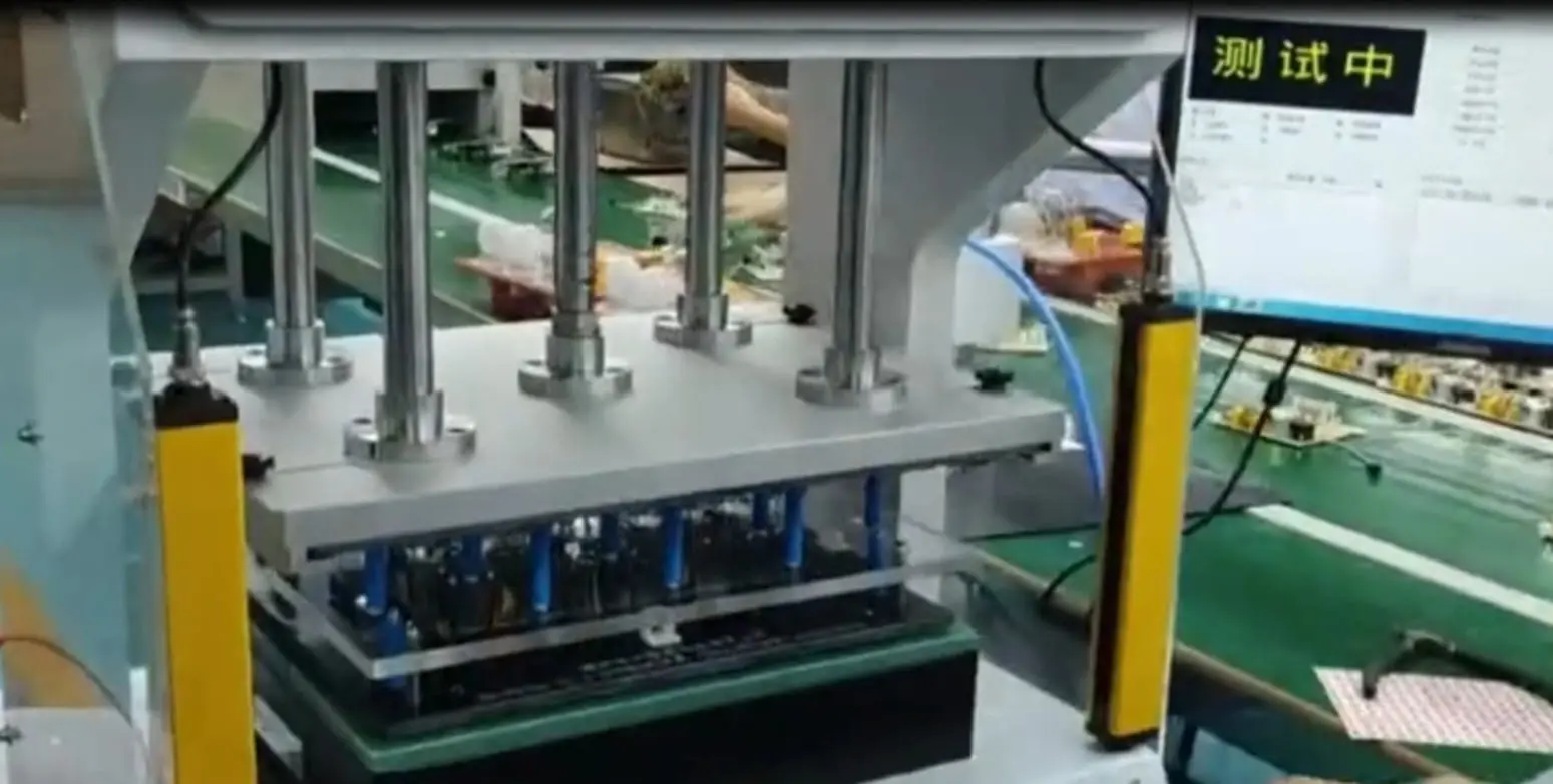
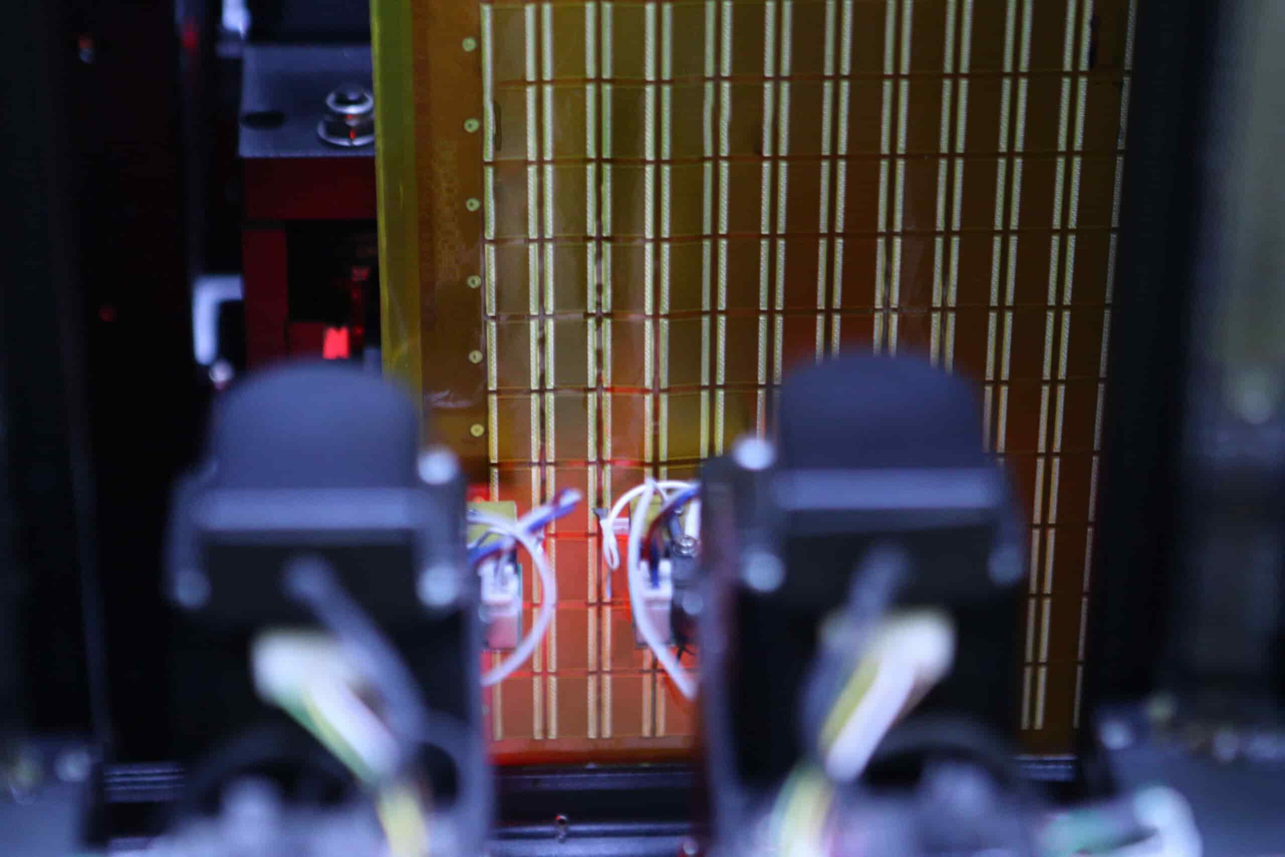
Bed of Nails Test
The Bed of Nails Test, also known as the in-circuit test (ICT) or pin-point test, is a more comprehensive and detailed test compared to the Flying Probe Test. It involves the use of a dedicated test fixture that contains a grid of spring-loaded pins, which make contact with specific test points on the PCB.
The Bed of Nails Test is typically employed for medium to high-volume production runs. The test fixture is custom-built to match the PCB layout, with the spring-loaded pins positioned to make contact with the designated test points. This test method allows for the measurement of various parameters, including analog and digital signals, and can provide more detailed information about the functionality and performance of the PCB.
Both the Flying Probe Test and the Bed of Nails Test are valuable tools in PCB testing, and the choice between them depends on factors such as production volume, test coverage requirements, and budget considerations. PCB designers should work closely with contract manufacturers to determine the most appropriate test method based on the specific needs of the project.
PCB DFT for Functional Circuit Testing
Highleap’s PCB Assembly Design for Testing (DFT) services encompass a holistic approach to ensure the functionality and quality of your printed circuit board assemblies (PCBAs). Our commitment to excellence in PCB testing draws from the best practices of both Functional Circuit Testing (FCT) and In-Circuit Testing (ICT).
DFT for Functional Circuit Testing
FCT represents a black-box approach, targeting the overall output and functionality of your PCBs. It emphasizes your specific test procedures rather than intricate board details. When you opt for FCT in your project, we initiate the process during the quoting stage. We encourage you to provide a written testing procedure, which we meticulously analyze to determine cost and lead time requirements. Streamlined FCT procedures can involve simple steps such as:
- Setting up the power supply.
- Activating the power supply.
- Validating specific messages on a display or the activation of designated LEDs.
Some clients incorporate LEDs in their designs explicitly to indicate correct operating voltages at specific board locations. While this approach may consume additional board space, it simplifies the testing process and reduces the need for extensive ICT.
DFT for In-Circuit Testing
ICT, on the other hand, adopts a white-box approach. Our testing engineers meticulously monitor individual voltage and current levels on completed PCBs, potentially executing step-by-step firmware procedures. ICT delves much deeper than FCT, requiring more time and resources. However, it excels at identifying potential issues on a PCB down to individual components.
ICT is most efficient for Prototype PCB Assembly projects, where lower order quantities minimize the impact of extended testing times. To optimize higher-quantity orders for ICT, you can design a testing fixture. This fixture streamlines testing by allowing us to quickly test PCB assemblies, similar to Bed of Nails PCB Testing for bare PCBs. Alternatively, including designated test points on the PCB assembly simplifies the probing process and improves efficiency.
At Highleap, we prioritize quality and functionality throughout our PCB Assembly Process. Multiple stages of testing, including E-Test, Visual Inspection, AOI, and AXI for lead-less components, are part of our default testing methods. Additionally, our clients have the flexibility to request additional testing methods, including ICT and FCT, depending on their specific requirements.
Our dedicated professional service team ensures that your concerns are addressed comprehensively. We meticulously evaluate Gerber and bill of material (BOM) files for Design for Manufacturing (DFM) and DFT checks. Communication with our team is seamless, with multiple available channels, including email, online forms, and attachments. Please share your concerns with us, and we will promptly provide an appropriate solution tailored to your unique PCB assembly needs.