RF and Microwave PCB
Highleap produces RF and Microwave PCB with multiple layers range from double-sided to the 20 layers, and the thickness range from 1oz to 6oz.
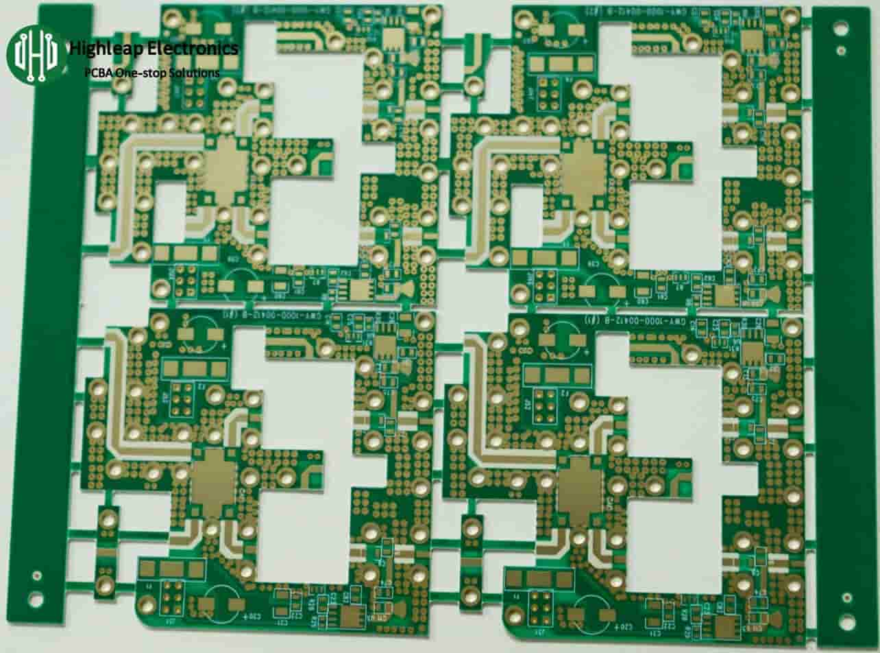
RF and Microwave PCB
RF(Radio Frequency) and Microwave PCBs are a specialized and advanced type of PCB specifically engineered to handle high-frequency signals ranging from Megahertz to Gigahertz.
An RF circuit board is generally defined as a high-frequency PCB that operates at frequencies above 100MHz.Within the radio frequency class, anything above 2GHz is a Microwave PCB.
RF circuit boards and Microwave PCBs are used for communication signals in any application that requires receiving and transmitting radio signals. For example, cell phones and radar installations.
Basic of RF and Microwave PCB
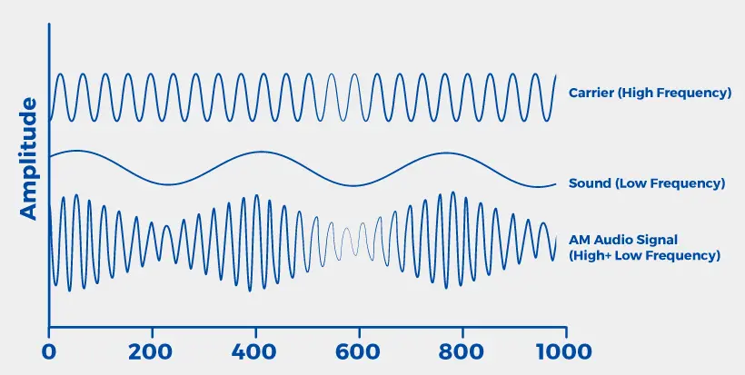
In essence, an electronic signal is a quantity that varies over time and communicates some kind of information. The quantity that varies is usually voltage or current. These signals are passed between devices as a way to send and receive information, like audio, video or encoded data. While these signals are often transmitted through wires, they can also be passed through the air by radio frequency, or RF, waves.
These radio frequency waves vary between 3 kHz and 300 GHz, but they are subdivided into smaller categories for the sake of practicality. These categories include the following:
Low-Frequency Signals
These are the signals handled by most traditional analog components, and they include signals with frequencies up to 50 MHz.
RF Signals
RF signals cover a wide frequency range, but in circuit design, they usually refer to frequencies from 50 MHz to 1 GHz, which are also used in AM/FM transmission.
Microwave Signals
Microwave signals have frequencies above 1 GHz, up to around 30 GHz. They are used for cooking in microwave ovens and high-bandwidth signal communication.
Applications for RF and Microwave PCBs
RF and microwave PCBs are used within the following applications and industries:
- Consumer electronics
- Military/aerospace
- High power applications
- Medical (X-ray)
- Automotive
- Industrial
Professional RF and
Microwave PCB Supplier
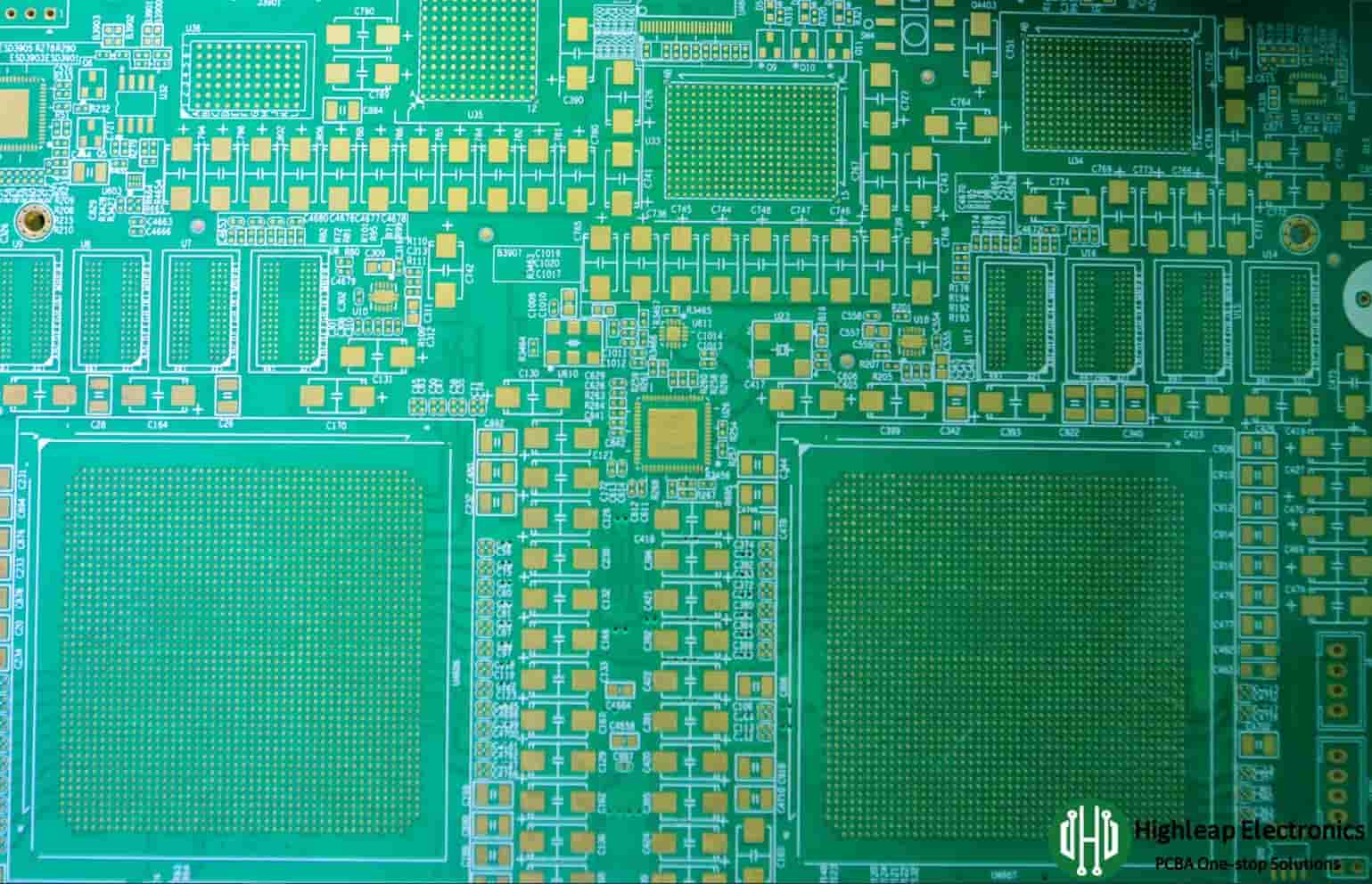
Highleap provides free one-on-one engineering support and DFX to RF and microwave PCBs projects.
Material for RF and Microwave PCB
RF and microwave PCBs are typically built using advanced composites with very specific characteristics for dielectric constant (Er), loss tangent, and co-efficient of thermal expansion (CTE).
RF and microwave PCBs‘ materials used in PCBs typically consist of a combination of PTFE , ceramics, hydrocarbon, and various forms of glass. The choice of material depends on factors such as quality, cost, ease of manufacturing, electrical performance, thermal robustness, and resistance to moisture.
Quality first
PTFE with microglass fiber or woven glass is often preferred. This material offers excellent electrical properties but may come at a higher cost. If budget constraints exist while maintaining high quality, ceramic-filled PTFE is a suitable alternative that provides good performance while being easier to manufacture, thereby reducing costs.
Cost concern
Ceramic filled with hydrocarbon is even more cost-effective to produce, but it may result in a slight decrease in signal reliability compared to other options.
Thermal robustness
Thermal robustness is crucial for applications exposed to soldering stresses, demanding drill scenarios in multilayer boards, or thermally challenging environments like aerospace. PTFE with microglass fiber or woven glass has excellent electrical properties but a high coefficient of thermal expansion (CTE). On the other hand, ceramic-filled PTFE offers great electrical characteristics and a low CTE, making it a thermally tougher choice. Ceramic-filled hydrocarbon sacrifices some electrical performance but maintains a very low CTE.
Moisture absorption
Moisture absorption is important to consider. PTFE ceramic has a lower rate of absorption, but adding woven glass can increase it. However, incorporating hydrocarbon in PTFE ceramic leads to a smaller increase in absorption, providing a balanced choice between cost and resistance to wet environments.
Consumer Electronics
Military/Space
High Power Applications
Medical
Automotive
Industrial
RF Materials
Bonding Materials
Attributes
Start your RF PCB Project!
Contact us directly to explore these options further and determine the best solutions for your RF PCB needs. Our team at Highleap is ready to assist you in achieving optimal results for your project.
The Guidelines for RF PCB Design
To ensure optimal performance of RF and microwave PCBs, it is important to follow certain design considerations:
1. RF Component Placement:
When designing an RF and microwave PCBs, digital designers should Carefully place RF components on the PCB to minimize signal loss and interference. Group related components together to reduce trace lengths and improve signal integrity.
2.Grounding and Power Distribution
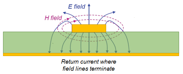
3.Transmission Line Design
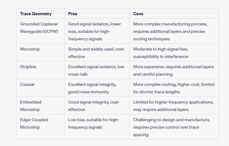
4.Routing and Trace Length
Keep RF and microwave PCBs traces as short and direct as possible to minimize signal loss and interference. Use wide traces to reduce resistance and inductance.
5.Noise Mitigation
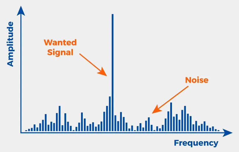
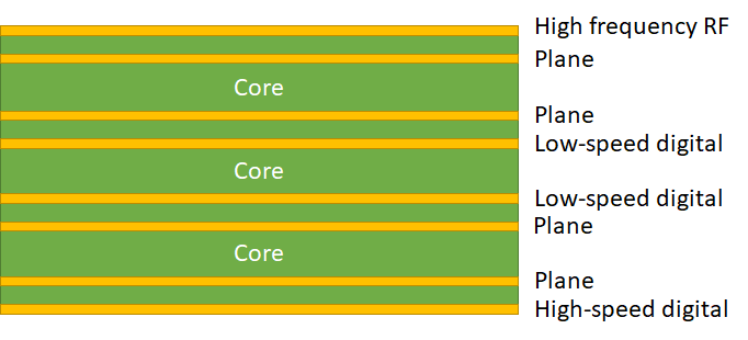
6.PCB Stack-up
Choose an appropriate RF and microwave PCBs stack-up that provides sufficient isolation and controlled impedance for RF and microwave signals. Consider using dedicated RF layers and separate power and ground planes.
7.EMI Shielding
8.Thermal Management
Impedance Matching
Impedance matching is another important requirement for RF and microwave PCBs.There are several things to keep in mind when you’re considering impedance matching in your design:
Skin Effect Loss
At higher frequencies, electrons will start to flow along the outer surface of the conductor. This is called a “skin effect.” At the trace, a small area is used to funnel electrons. However, this funnel also traps some of the electrons flowing on the outside of the conductor, converting their signal energy into heat. This is what is called “skin effect loss.” This loss is best minimized with proper impedance matching and even PCB plating with gold.
Keep Line Lengths Low
The longer the lines that carry RF and microwave signals, the more chance there is for signal loss. Ideally, the line should be 1/20 of the wavelength. If it needs to be longer than 1/16 of the wavelength, also called the critical signal length, you’ll need to apply impedance control to that trace with L and C components to the end of the line.
Looking for PCBs Quote?

Full Expertise
We have a superior engineer team, which supports person-to-person services.

Fast Lead Time
We have faster lead time about 48 hours for some PCBs prototypes

Strict Quality Control
We ensure strict quality control measures in every production process.
Take a Quick Quote
Discover how our expertise can help with your next PCB project.

