Schematic Diagram for PCB
Based on your design requirements, let ‘s create the schematic diagram.

What is PCB Schematic Diagrams
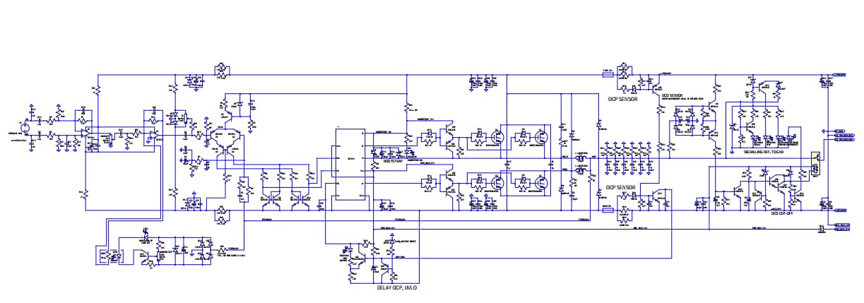
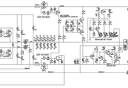
Schematic diagrams serve as a blueprint for designing and manufacturing electronic circuits. A PCB Schematic Diagram is a graphical representation of an electronic circuit, showcasing the arrangement of components and connections. They provide a visual guide for engineers, allowing them to understand and work with complex circuits.
Schematic Diagram vs. PCB Layout

Schematic Diagram
Focuses on the logical connections between components.

PCB Layout
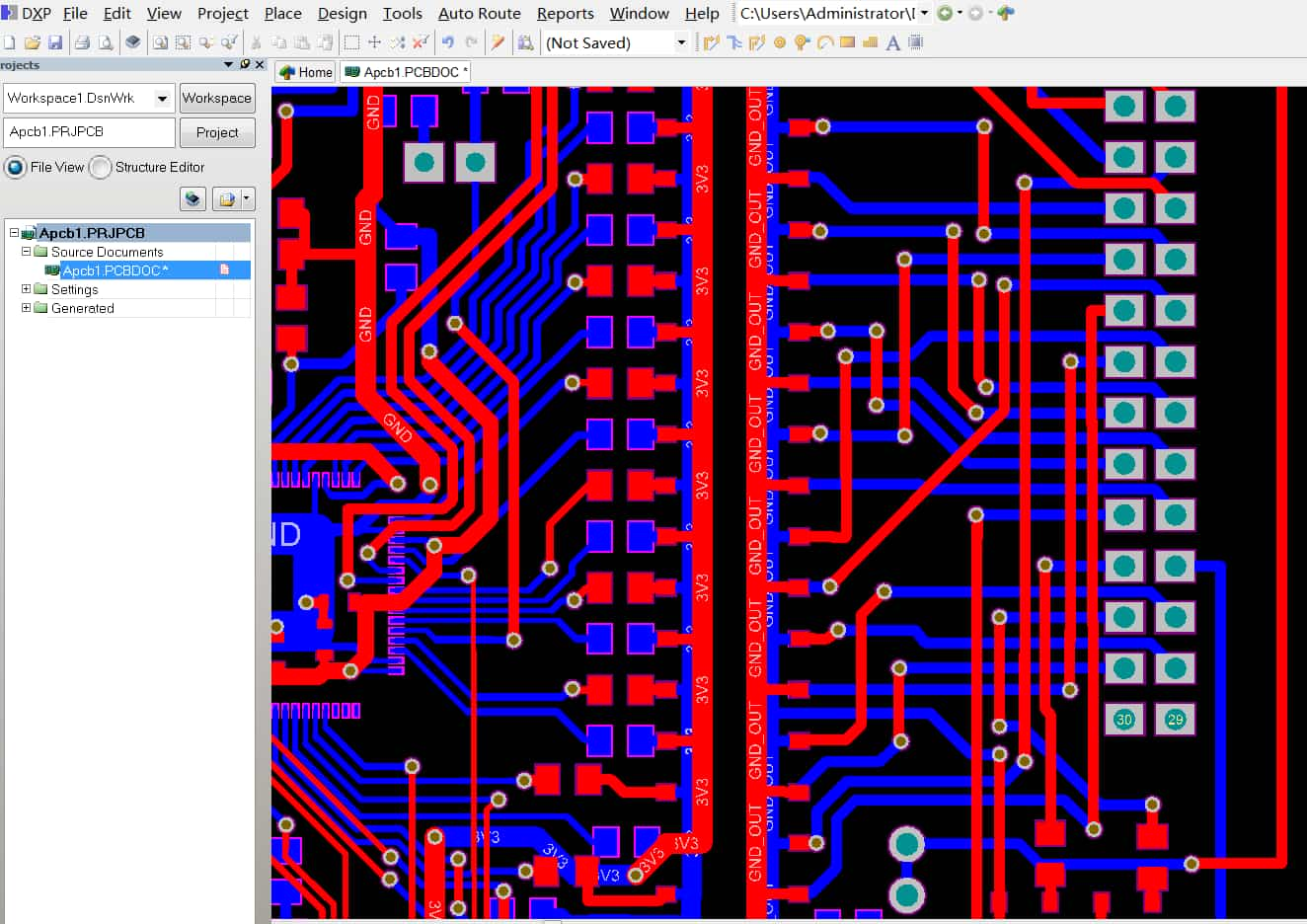
Deals with the physical arrangement of components on the actual board.
Delve into the importance of schematic diagrams:
Schematic diagrams serve as a visual representation of complex electronic circuits. They simplify the understanding of a circuit’s functionality, making it easier for engineers, designers, and technicians to grasp the connections between various components.
Furthermore, schematics are invaluable tools for diagnosing and rectifying issues in electronic circuits. When a circuit malfunctions, engineers can refer to the schematic to identify the source of the problem quickly. This expedites the debugging process, reducing downtime and costs.
How to Create a Schematic Diagrams
Select the Right Software
Choose a PCB design software that suits your needs. Some popular options include Eagle, Altium Designer, KiCad, OrCAD, and EasyEDA. These tools offer libraries of components and features for schematic capture.
Page Naming Convention
A_Block Diagram
B_Power Supply
C_MCU Interface
D_Memory Interface
E_Revision History
Grid Setting
Configure the grid settings in your design software. Use a grid that aligns with your components’ sizes and pin spacing for precise placement.
Page Title Block
Notes/Comments:
Revision History
Block Diagram
Hierarchical Schematic Design
Component Referencing
Symbol Generation
Create or use predefined symbols for components. Ensure symbols accurately represent the actual components in the design.
Net Connections
DRC Check (Design Rule Check)
Run a DRC check to identify and rectify design rule violations, such as improper clearances or unconnected nets.
How to Convert PCB to Schematic Diagram
Engineers often face challenges when it comes to locating the necessary drawings for repairing older electronic products. Drawing circuit diagrams becomes essential for product analysis and improvement, and this process involves several key steps:
1
Selecting Key Components
Start by carefully choosing integrated circuits, transformers, transistors, and other crucial electronic components, especially those with numerous pins, as they play pivotal roles in the process.
2
Selecting Key Components
If the PCB has element numbers marked, these sequential numbers follow specific rules. Utilize this numbering system as a reference point when drawing the PCB layout.
3
Manual Numbering
In cases where serial numbers are absent on the printed board, it becomes necessary to assign numbers manually. This facilitates inspection and editing tasks.
4
Distinguishing Wire Types
Properly differentiate the grounding, power, and signal wires on the printed board.
5
Interleaved Wiring
In order to avoid overcrowding, circuit diagram wiring is often interleaved, leading to complex visuals. You can simplify this by using terminal marks and grounding symbols for power supply and grounding wires. For circuits with numerous components, consider drawing unit circuits separately and then integrating them.
6
Drawing Tools
When sketching, opt for transparent tracing paper and color pens for clarity. Differentiate components with colors (e.g., ground wires, power cables, signal cables) for easy visual recognition and quick circuit analysis.
7
Mastering Unit Circuits
Designers should have expertise in unit circuit elements and classical drawing techniques, such as rectifier bridges, voltage stabilization circuits, operational amplifiers, and digital integrated circuits.
8
Reference Circuit Diagrams
When drawing the circuit diagram, seek out circuit diagrams from similar products for reference. This practice can significantly streamline the drawing process, making it more efficient.
Take a Quick Quote
Discover how our expertise can help with your next PCB project.
