PCB Layout
Expert PCB Layout Services for Your Designs.

Precision PCB Layout
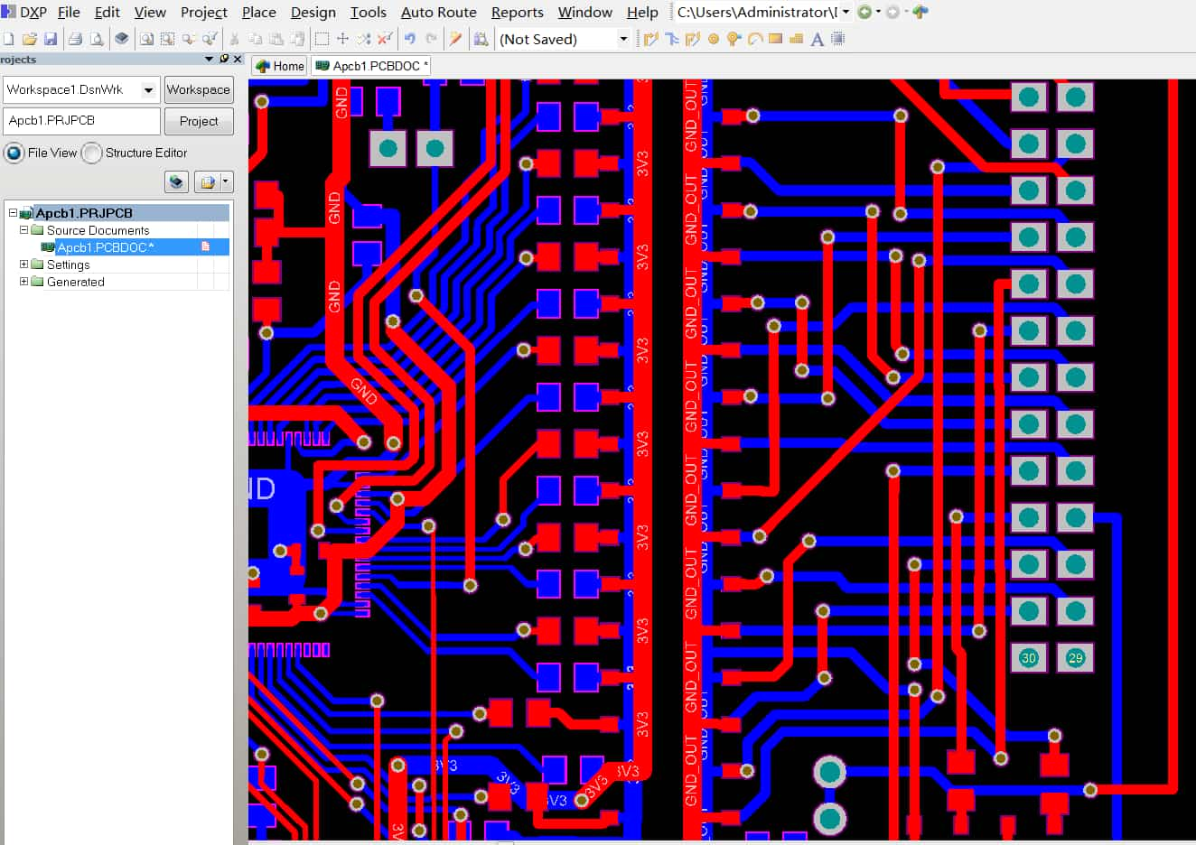
At Highleap Electronic, we understand that PCB layout is the foundation of every successful electronics project. It’s the intricate dance of components, traces, and connections that bring your design to life. With our advanced PCB layout services, we meticulously transform your schematic into a functional and efficient circuit board, ensuring optimal performance and manufacturability.
A Schematic Diagram to PCB Layout
In the past, schematic drawings and PCB layouts were meticulously hand-crafted, and those skilled in these arts were highly sought after. However, in today’s age, ECAD tools have revolutionized the creation of these PCB diagrams. Transitioning from a schematic to a PCB layout has become an automated process facilitated by computer software.
1
Choose the Circuit Board Dimensions
Commence the process by selecting the appropriate dimensions for the circuit board. While most ECAD tools offer preset board sizes and customizable options for area and thickness
2
Formulate the Stack Configuration
After defining the board size, materials, layer count, and type, proceed to establish the stack configuration. This foundational step lays the groundwork for the subsequent design process.
3
Arrange Component Placement
Efficiently organizing components is the next pivotal step. Post partitioning and adhering to licensing rules, position the components on the board. This meticulous arrangement is fundamental to the successful construction of the board.
4
Navigate Routing and Tracing
Routing and tracing entail wiring, a task often considered the most intricate in PCB layout. This complexity intensifies in the case of multi-layer boards with a significant number of vertical through-holes (PTH) that transmit signals internally and to the ground plane. Adhering to proper spacing and gap regulations during track routing is crucial.
5
Conduct Thorough Checks
Before finalizing the PCB design, it’s essential to perform meticulous checks for any errors. Integrate a Design Rule Check (DRC) assessment to verify if your design aligns with the prescribed layout guidelines and restrictions. These regulations should align with the CM’s Design for Manufacturability (DFM) guidelines to ensure manufacturability.
PCB Layout Software
Our PCB layout services are powered by the latest and most advanced design software. This ensures that potential issues are addressed early in the design process, minimizing the need for costly revisions later.
Altium
Altium offers extensive libraries of components, reducing the time spent on creating footprints and symbols. Engineers can visualize the PCB design in 3D, aiding in identifying potential clearance issues.
Cadence Allegro
Allegro excels in handling complex designs with high layer counts and advanced routing requirements. And it also supports team collaboration by allowing multiple engineers to work on different parts of the design simultaneously.
Mentor Graphics PADS
PADS provides tools for high-speed design, including differential pairs and impedance control. Engineers can seamlessly integrate their designs with simulation tools for validation and optimization.
EAGLE
EAGLE’s integration with Autodesk Fusion 360 enables collaboration between electronics and mechanical design teams.
AutoCAD
AutoCAD’s 3D modeling capabilities can be useful for incorporating mechanical elements into the PCB design.
OrCAD
Engineers can perform circuit simulations for analog, digital, and mixed-signal designs. And OrCAD supports a wide range of design sizes, from simple to complex, accommodating various project requirements.
Capabilities of PCB Layout
We possess the capability to set up digital, analog, and mixed-signal technologies, ensuring controlled impedance, matched-length pairs for DDR, RF layout, and high-speed signals reaching beyond 100 GHz. Our expertise extends to all types of PCB structures, encompassing:
- Rigid PCB
- Rigid-flex PCB
- Rigid PCB
- Hybrid PCB
- BGA/micro BGA
- Blind vias
- Buried vias
- High-Density Interconnect(HDI)
Main Services
Items
Capabilities
Advantages of Highleap’s Layout Services

Expertise
Our layout engineers are experts in their field, ensuring that your design is optimized for performance, manufacturability, and reliability.

Efficiency
Our dedication to respect for the individual isn’t just a statement; it’s a lived reality.We cultivate a culture where the spark of each individual’s potential ignites a brighter future.

Prototyping
We provide prototypes for rigorous testing, giving you the confidence that your design will function flawlessly in real-world scenarios.

Flexible
Whether it’s a complex multilayer design or a compact single-layer board, we tailor our services to your project’s specific needs.
Take a Quick Quote
Discover how our expertise can help with your next PCB project.
