Professional FR4 PCB Manufacturer

Highleap provide good quality FR4 PCB manufacture up to 60 layers, whether prototype or mass production.

What is FR4 PCB?

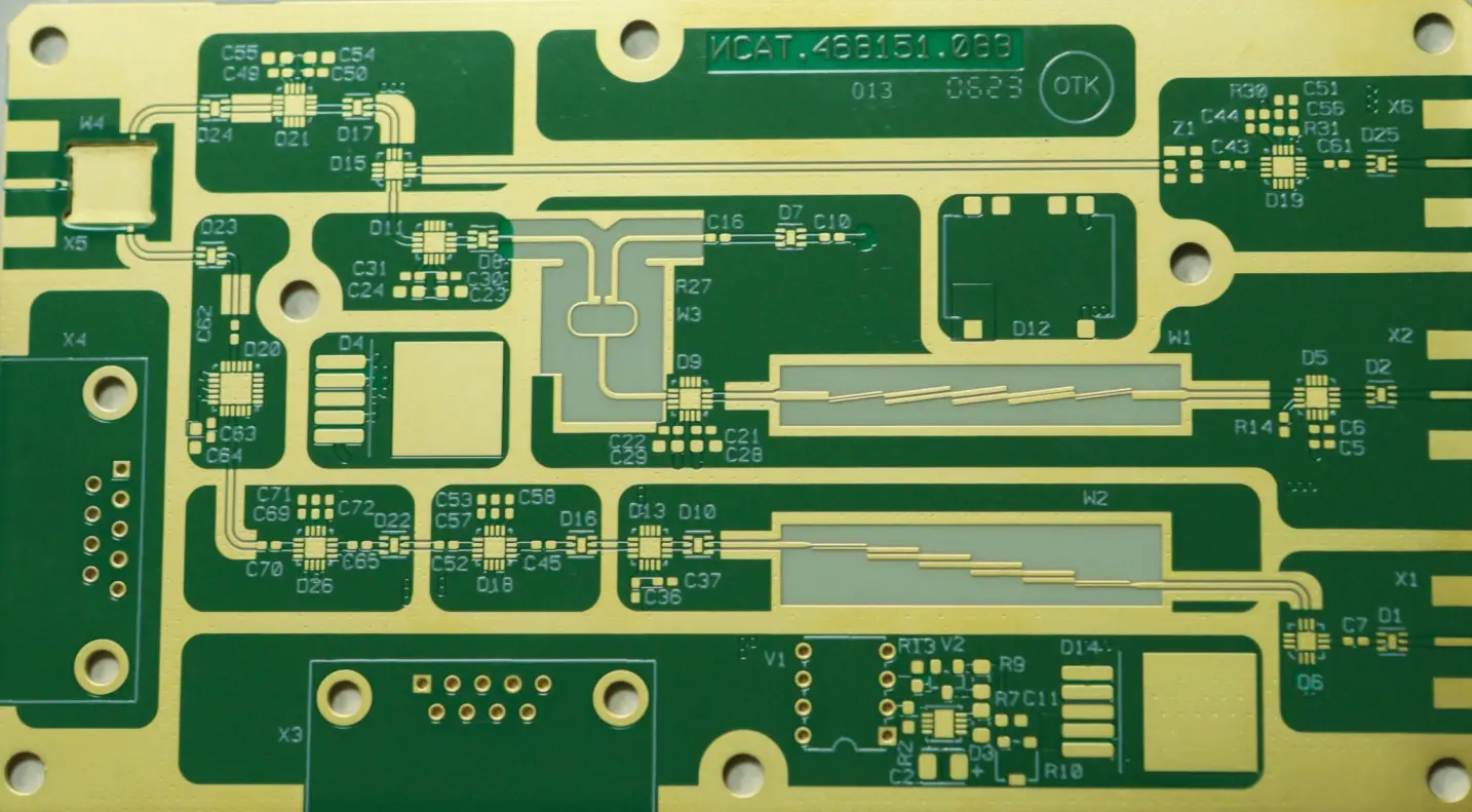
FR4  is a common dielectric material used in printed circuit boards. It stands for fiberglass-reinforced epoxy-laminated sheets, providing mechanical support and separating copper layers.
The “FR” in FR4 indicates flame retardant, meeting UL94V-0 standard for inflammability. It prevents fire expansion and ensures immediate extinguishing when burning.
A print circuit board with FR4 is called the FR4 PCB.The FR4 sheets are combined with copper layers on both sides to form a Copper Clad Laminate (CCL). FR4 provides strength and durability to PCB boards, making them reliable for various applications.
HF-PCB

Why Highleap Electronic is the Preferred Partner for FR4 PCB Manufacturing and Assembly

Highleap Electronic stands out as a leading provider of FR4 PCB manufacturing and assembly, combining advanced technology, rigorous quality control, and flexible, customer-focused solutions. Here are the key advantages:

  1. Advanced Manufacturing: Utilizing state-of-the-art equipment, Highleap Electronic ensures precise material cutting, accurate LDI positioning, and controlled plating processes—whether through pattern plating or negative electroplating—resulting in FR4 PCBs with superior electrical performance.

  2. Rigorous Quality Control: Comprehensive inspection protocols, including AOI, impedance testing, and final functional checks, ensure each board meets strict international standards.

  3. Customization and Flexibility: Highleap Electronic offers tailored solutions for a wide range of FR4 PCB applications, including boards with enhanced thermal and electrical properties, and supports various surface finishes such as HASL and ENIG.

  4. Efficient Turnaround: With optimized processes and streamlined production, Highleap Electronic delivers high-quality PCBs with competitive lead times and cost efficiency.

  5. Comprehensive Assembly Solutions: Beyond manufacturing, the company provides complete PCB assembly services, ensuring precise component placement and robust soldering for a fully integrated solution.

Highleap Electronic’s commitment to innovation and quality has earned the trust of global electronics manufacturers. For more information on their services, please visit:

PCB FR4
FR4 PCB

Searching FR4

PCB Supplier?

Being a trusted rigid fr4 printed circuit board manufacturer with a vast industry experience, we specialize in all kinds of printed circuit boards.
Are you searching for a manufacturer to meet your  PCB needs? Look no further than Highleap!

Properties of FR4 PCB

Why choose FR4 material as material for your PCB project? The following may be the answer.

Flame Retardant

FR4 is the standard material for PCBs, known for its fire-resistant properties. It consists of a fiberglass-reinforced epoxy laminate with Bromine, a halogen element known for flame-retardant characteristics. This combination helps prevent or delay fire spread during electrical faults.

Low-Cost

FR4  material offers a cost-effective solution for a wide range of applications. However, it’s important to note that FR4 materials with specific properties such as a high glass transition temperature or high comparative tracking index may come at a slightly higher price.

Load Bearing

As we know that FR4 is a combination of fiberglass and epoxy resin, and it provides high load-bearing capacity and mechanical strength to the overall PCB.
But mainly, the strength and load bearing depend on the thickness of the material. The thickness of a standard FR4 material varies between 0.2 to 3.2m

Higher Glass Transition Temperature

FR4  pcb is known for its high temperature resistance, typically offering a Tg (glass transition temperature) value of 150°C or 170°C.
By using FR4 with a high Tg value, manufacturers can ensure that their PCBs can withstand higher temperatures, resist moisture absorption, and exhibit enhanced chemical resistance.

Excellent Electrical Properties

The FR4 is used as the base material which makes its electrical properties important to be noticed. As the electrical properties of a PCB material are crucial for signal integrity, impedance control, and the quality of insulation.
However, FR4 isn’t the best material for high-frequency applications since it has a more wondrous Df (dissipation factor) than high-frequency materials.

High Dielectric Strength

FR4 material provides high dielectric strength somewhere between 4.25-4.55.
However,FR4 does not offer uniform dielectric constant like high-speed board materials.As the frequency goes up the Dk varies. Dielectric constanttolerances for high-speed materials are less than 2%, whereas for FR4 it is up to 10%.

Moisture Resistant

FR4 PCBs have excellent moisture resistance, making them ideal for various applications, even in humid and marine environments. Manufacturers enhance moisture resistance through techniques like protective coatings and moisture-resistant additives.

Higher Decomposition Value

The decomposition temperature (Td) defines the temperature where a PCB’s almost 5% of the laminate’s mass is lost due to decomposition. FR4 PCB material provides a higher decomposition temperature of 345 Celsius.
FR4 PCB Manufacturing Suggestions

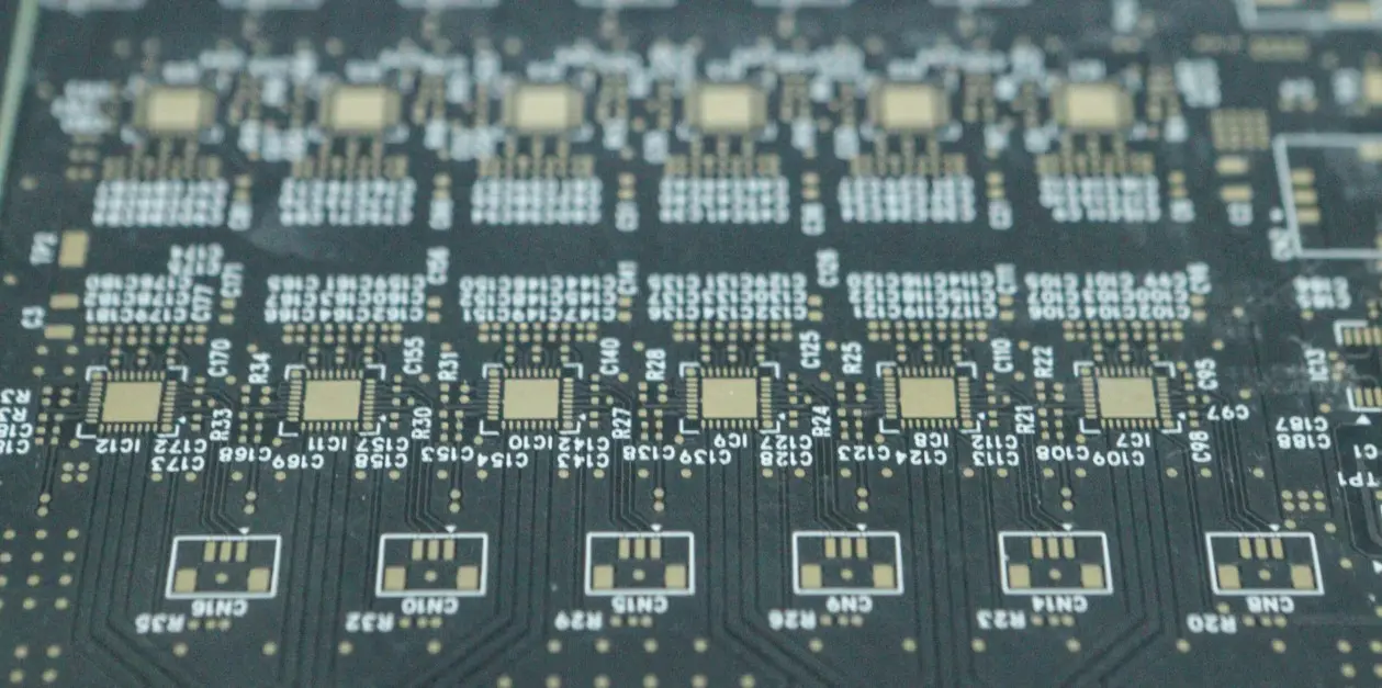
When considering FR4 as the base material for your PCB, several key factors must be evaluated to ensure optimal performance, manufacturing efficiency, and cost-effectiveness for your specific project needs. These factors include thickness and weight, flexibility options, impedance control, and temperature management.

1. Thickness and Weight

Modern FR4 thickness ranges from 0.1mm to 6.0mm (according to IPC-4101E standards). For wearable electronics like smartwatches, ultra-thin boards (0.1–0.4mm) are suitable but must be designed with symmetric lamination to avoid warping. The standard thickness (1.6mm) is commonly used for consumer electronics, offering a good balance of performance and cost. Thicker FR4 boards (over 3mm), now 15% lighter due to fiberglass optimization, are used in high-power applications like electric vehicle charging stations.

2. Flexibility and Thermal Management

Flexibility is critical for applications like medical devices and automotive electronics. Thinner FR4 boards provide flexibility but may be more prone to warping during soldering. For high-power and high-heat applications, high thermal conductivity FR4 (Tg180+ and TD ≥1.2W/mK) offers superior heat dissipation, allowing FR4 to replace up to 60% of aluminum-based boards, reducing costs by 40% while maintaining performance.

3. Controlled Impedance and Signal Integrity

For high-frequency applications, FR4 variants with low Dk/Df materials, such as Isola 370HR, are now available with a Dk of 3.8 at 10GHz, providing improved signal integrity. These materials are ideal for 5G and high-speed circuits, ensuring stable performance at 28GHz. Advanced designs often rely on these materials to manage impedance control, which is critical for high-speed signal transmission.


FR4 Circuit Board

Start Your FR4 PCB Project!

Highleap specializes in the FR4 PCBs manufacturing more than 10 years.We have a strong capacity and can produce various FR4 PCBs.Send your request now!

Capabilities of Manufacturing

We provide the PCB in various surface finishing options,such as

  • Gold Fingers
  • HASL (Hot Air Solder Leveling)
  • ENIG (Electroless Nickel immersion Gold)
  • OSP (Organic Solderability Preservatives)
  • Immersion silver
  • Immersion tin,and so on

The boards are available in all leading solder mask colors, such as white, blue, black, green, and red.

Circuit Board
Items
Max Layer
Inner Layer Min Trace/Space
Out Layer Min Trace/Space
Inner Layer Max Copper
Out Layer Max Copper
Min Mechanical Drilling/Annular Ring
Min Laser Drilling/Annular Ring
Aspect Ratio(Mechanical Drilling)
Aspect Ratio(Laser Drilling)
Press Fit Hole Tolerance
PTH Tolerance
NPTH Tolerance
Countersink Tolerance
Board Thickness
Board Thickness Tolerance(<1.0mm)
Board Thickness Tolerance(≥1.0mm)
Impedance Tolerance
Min Board Size
Max Board Size
Contour Tolerance
Min BGA
Min SMT
Surface Treatment
Solder Mask
Min Solder Mask Clearance
Min Solder Mask Dam
Legend
Min Legend Width/Height
Strain Fillet Width
Bow & Twist
Capabilities
60L
2/2mil
2/2mil
10oz
10oz
0.15mm/0.127 mm
0.075mm/0.075 mm
20:1
1:1
±0.05mm
±0.075mm
±0.05mm
±0.15mm
0.4-8mm
±0.1mm
±10%
Single-Ended:±5Ω(≤50Ω),±7%(>50Ω)
Differential:±5Ω(≤50Ω),±7%(>50Ω)
10*10mm
22.5*30inch
±0.1mm
7mil
7*10mil
ENIG,Gold Finger,Immersion Silver,Immersion Tin,HASL,OSP,ENEPIG,Flash Gold;Hard gold plating
Green,Black,Blue,Red,Matt Green
1.5mil
3mil
White,Black,Red,Yellow
4/23mil
/
0.3%

Types of FR4 PCB

FR4 can be broadly classified into the following types. Choose the appropriate FR4 type based on your specific requirements.

Standard FR4 PCB

Standard FR4 refers to the conventional fiberglass-reinforced epoxy laminate with a heat resistance of approximately 150–160°C. It is widely used due to its excellent electrical insulation properties, mechanical strength, and cost-effectiveness. Standard FR4 PCBs are suitable for general electronic applications with moderate thermal and electrical requirements.

High-TG FR4 PCB

High-TG FR4 features a higher glass transition temperature (TG), typically 170°C or above. While standard FR4 provides good insulation and flame resistance, its thermal and electrical stability may degrade under high power, voltage, or temperature conditions. High-TG FR4 is designed for applications requiring enhanced heat resistance, such as automotive, industrial, and high-power electronic circuits.

High-CTI FR4 PCB

The Comparative Tracking Index (CTI) measures a material’s ability to withstand electrical tracking, which occurs due to leakage currents over time. A higher CTI value (up to 600V) provides improved resistance to electrical breakdown in harsh environments. High-CTI FR4 is commonly used in high-voltage and high-reliability applications where insulation performance is critical.

FR4 PCB Without Copper Lamination

FR4 substrates without laminated copper differ from standard FR4 PCBs in that they do not include a conductive copper layer. These boards are primarily used for insulation, mechanical support, and structural applications, such as mounting other PCB components or serving as electrical barriers within assemblies.

Highleap Electronic’s FR4 PCB Manufacturing Process

At Highleap Electronic, we are dedicated to producing high-quality FR4 printed circuit boards (PCBs) through a reliable, industry-standard manufacturing process. Our process integrates advanced technologies with rigorous quality control to meet the exacting demands of modern electronics. For standard FR4 PCBs, we typically follow two primary manufacturing processes. Below is an example of our multilayer PCB process, utilizing negative electroplating (for pattern definition) and HASL/ENIG surface finishes:

Example with Negative Electroplating and HASL/ENIG:

Material Cutting → Post-Cutting Material Drying → LDI Hole Positioning → Inner Layer Dry Film Application → Inner Layer Etching → Inner Layer AOI Inspection → Browning Treatment → Lamination → Drilling (including aluminum drilling) → Metallization Milling → Deburring → Copper Plating → Negative Electroplating → Negative Electroplating Grinding → Negative Dry Film Application → Dry Film Inspection → Negative Etching → Outer Layer AOI Inspection → Surface Grinding → Solder Mask Hole Filling → Solder Mask Application → Solder Mask Inspection → Silkscreen Printing → HASL/ENIG Surface Finish → Impedance Testing → Electrical Testing → Secondary Drilling, V-CUT → Routing → Functional Testing → Final Inspection → Packaging → Finished Goods Storage.

Note: If a large tin area is present in the silkscreen section, tin plating should be applied before silkscreen printing to ensure proper adhesion and clarity.

Example with HASL/ENIG via Pattern Plating:

Material Cutting → Post-Cutting Material Drying → LDI Hole Positioning → Inner Layer Dry Film Application → Inner Layer Etching → Inner Layer AOI Inspection → Browning Treatment → Lamination → Drilling (including aluminum drilling) → Metallization Milling → Deburring → Copper Plating → Pattern Plating → Pattern Plating Grinding → Dry Film Stripping → Dry Film Inspection → Pattern Etching → Outer Layer AOI Inspection → Surface Grinding → Solder Mask Hole Filling → Solder Mask Application → Solder Mask Inspection → Silkscreen Printing → HASL/ENIG Surface Finish → Impedance Testing → Electrical Testing → Secondary Drilling, V-CUT → Routing → Functional Testing → Final Inspection → Packaging → Finished Goods Storage.

Note: When large tin areas are found in the silkscreen section, tin plating should be applied before silkscreen printing to ensure proper adhesion and clarity.

FR4 PCBs

Comparison of Negative Panel Plating and Pattern Plating in PCB Manufacturing

In PCB manufacturing, Negative Panel Plating and Pattern Plating are two distinct electroplating methods, with fundamental differences in process flow, material consumption, and application scope. Below is a technical comparison of the two processes:

1. Process Principle Comparison

The core difference between these two methods lies in the way copper is applied and removed. Negative Panel Plating is a subtractive process where the entire panel is initially plated with copper, followed by etching to remove excess copper and form the desired circuitry. In contrast, Pattern Plating is an additive process where copper is selectively plated only in the pattern areas, and the remaining copper is not plated.

In Negative Panel Plating, a dry film negative is used as the mask, which retains the exposed areas after development. The copper layer is plated across the entire board to a target thickness, followed by etching to remove the excess. On the other hand, Pattern Plating uses a positive wet film mask, which removes the exposed areas after development. The process involves plating a thin copper layer onto the substrate before selectively thickening the copper in the desired pattern areas.

2. Process Flow Differences

The typical process flow for Negative Panel Plating begins with drilling, followed by a full-board copper electroplating step. After that, a dry film is applied and exposed to create the negative image, followed by development, etching, and de-masking before proceeding to subsequent steps.

In contrast, the Pattern Plating process starts with drilling and the application of a thin copper layer. After applying the wet film, the positive exposure and development steps are performed, followed by pattern electroplating to thicken the copper only in the selected areas. After de-masking, the base copper layer is etched away, and the remaining process steps follow.

3. Key Technical Parameter Comparison

When comparing the two processes, several critical parameters stand out. For example, the minimum trace width and spacing are typically 3/3 mil for Negative Panel Plating, with an extreme limit of 2/2 mil. Pattern Plating offers slightly better precision, with a typical 2/2 mil and an extreme limit of 1/1 mil.

In terms of copper thickness uniformity, Negative Panel Plating can achieve a uniformity of ±15%, influenced by current distribution, while Pattern Plating offers more precise control with ±8% uniformity. Additionally, side-etching control is greater in Pattern Plating (≤5μm), ensuring more vertical edges, compared to Negative Panel Plating (10-15μm), which can cause mushrooming effects at the edges.

4. Cost and Efficiency Analysis

In terms of material cost, Negative Panel Plating consumes a higher amount of copper, with an additional 150-200g of copper per square meter, and requires a large quantity of etching solution. In comparison, Pattern Plating reduces copper consumption by over 30%, making it a more cost-efficient option for high-precision and fine-line PCBs.

For equipment investment, Negative Panel Plating requires large electroplating tanks (10,000L or more), keeping equipment costs relatively low. On the other hand, Pattern Plating requires pulse plating machines with high precision (±3ASD), resulting in equipment costs that are 30-50% higher.

Regarding environmental impact, Negative Panel Plating generates wastewater with a high copper content (8-12g/L), leading to higher treatment costs. Pattern Plating, however, generates wastewater with a lower copper content (2-5g/L), making it more environmentally friendly and compliant with RoHS standards.

Both Negative Panel Plating and Pattern Plating have their unique advantages and are chosen based on the specific requirements of the PCB design. Negative Panel Plating is more cost-effective for large-scale production with simpler designs, but Pattern Plating offers higher precision and lower environmental impact, making it ideal for high-precision applications and high-end electronics. The choice between the two processes depends on factors such as the required line width, application, and overall production cost.

Why FR4 is the Most Popular PCB Material

FR4’s dominance in the PCB market can be attributed to its unique combination of properties, making it suitable for a variety of electronic products. Here’s why FR4 is so widely favored:

  • Cost-Effective Solution – Compared to specialized materials like ceramic or PTFE, FR4 offers a good balance of affordability and performance, making it ideal for mass production.
  • Excellent Electrical Insulation – FR4 provides stable insulation properties, ensuring that signal transmission is reliable and consistent for most standard applications.
  • Mechanical Strength – The fiberglass reinforcement in FR4 provides durability, impact resistance, and resistance to bending, allowing it to perform well in tough environments.
  • Easy to Process – FR4 is relatively easy to process with common PCB manufacturing techniques like drilling, lamination, and etching.
  • Flame Retardant – FR4’s flame retardant nature ensures that the PCB does not catch fire under extreme conditions, improving the safety of electronic devices.
FR4 PCB

Exploring Alternatives to FR4 in PCB Materials

FR4 has long been the go-to material in PCB manufacturing, known for its affordability, reliability, and versatility in various general-purpose applications. However, as technology advances and circuit requirements become more specialized, the limitations of FR4 become more apparent. With the increasing complexity of modern electronics, alternatives to FR4 are becoming more essential for addressing the unique needs of high-performance circuits.

The Limitations of FR4

While FR4 is a solid choice for basic circuit designs that operate at low frequencies and in non-extreme conditions, it is not without its drawbacks. One of the main limitations of FR4 is its low thermal conductivity, which makes it unsuitable for high-temperature environments. Additionally, FR4 struggles in high-frequency circuit designs due to its fluctuating dielectric constant (Dk) and high dissipation factor (Df), both of which can cause signal loss and reduced performance in sensitive applications. Moreover, FR4 does not provide controlled impedance, a crucial requirement for many high-speed and high-frequency circuits, such as those used in telecommunications or computing.

Why Consider FR4 Alternatives?

Not all circuits are created equal, and not all applications demand the same set of characteristics. This is where alternatives to FR4 come into play. For designs that require high heat resistance, better signal integrity, or consistent performance at higher frequencies, alternative materials can offer much-needed benefits. High-performance circuits—such as those found in aerospace, telecommunications, and medical devices—need materials that can handle more extreme conditions than what FR4 can offer. In such cases, exploring other options ensures that circuit designs meet stringent specifications without compromise.

High-Performance PCB Materials

As the demand for advanced circuit boards increases, several materials have emerged as alternatives to FR4, each offering its own set of benefits:

  • Metal-Core PCBs (MCPCBs): For designs where heat dissipation is critical, Metal-Core PCBs (MCPCBs) are an excellent alternative. Typically made with aluminum or copper as the base material, MCPCBs are ideal for applications with high thermal requirements, such as LED lighting, automotive circuits, and power supplies. Aluminum-based MCPCBs are cost-effective, while copper-based MCPCBs offer superior thermal conductivity for even more demanding applications.

  • PTFE (Polytetrafluoroethylene): PTFE is another great alternative, particularly for high-frequency applications. Known for its low signal loss, stable dielectric properties, and high thermal stability, PTFE is perfect for RF (radio frequency) and microwave circuits. This material excels in minimizing signal degradation, making it a go-to for high-speed, high-frequency designs in industries like telecommunications and aerospace.

  • Ceramic PCBs: For power electronics and applications requiring excellent thermal management and high temperature resistance, ceramic-based PCBs are ideal. While more expensive and complex to manufacture than FR4, ceramic PCBs offer exceptional thermal conductivity, high voltage resistance, and long-term reliability, making them well-suited for military, medical, and high-end industrial applications.

Tailoring the Right Material to Your PCB Needs

The choice of PCB material ultimately comes down to the specific requirements of the application. For industries like automotive and lighting, where thermal management is paramount, MCPCBs deliver superior heat dissipation. For high-frequency and high-speed applications, such as in telecommunications and high-performance computing, PTFE ensures stable signal integrity. For robust, high-temperature applications in critical industries like defense and medical devices, ceramic PCBs provide the durability and reliability needed.

At Highleap Electronic, we understand that every circuit board is unique and requires careful consideration of materials to meet performance and environmental needs. We offer a wide range of PCB solutions, from standard FR4 to advanced alternatives like MCPCBs, PTFE, and ceramic PCBs. Our team of experts is here to help you select the best material for your application, ensuring optimal performance and long-term reliability. Whether you’re designing a high-frequency circuit or managing heat in power applications, we have the right solution for you.

As the demand for more specialized PCB materials grows, we remain committed to providing our customers with the highest quality products tailored to their specific needs. Let us help you bring your designs to life with the perfect PCB material that meets both your technical specifications and your budget.

Choose Highleap as Your PCB Manufacturer

icon

Full Expertise

We have rich experience in all kinds of PCB manufacturing and assembly.From component procurement to product delivery, we can complete every step with high quality.

icon

Strong Supplier Network

With 10 years of experience in the PCB industry, Highleap owns a supplier network that provides us with reliable access to get high-quality components at competitive prices.

icon

Strict Quality Control

At each process, we strictly control the quality by implementing a variety of testing and inspections to ensure that each PCBA reaches the highest quality standard.

Take a Quick Quote

Discover how our expertise can help with your next PCB project.