High Frequency PCB
If you’re looking to optimize your wireless networks or applications that rely on seamless signal transmission, investing in high frequency PCBs is a smart choice.
What’s High Frequency PCB
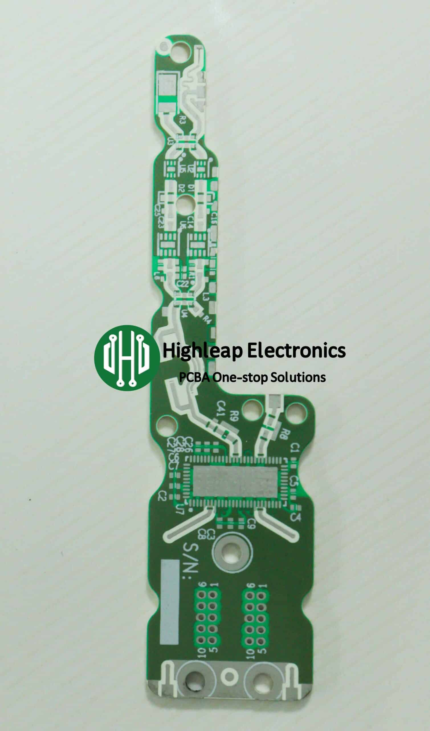
High frequency PCBs,referred to as HF PCBs,are used to transmit electromagnetic waves in the frequency of GHz with minimal loses . These PCBs come in a frequency range of 500MHz to 2GHz.HF PCBs are defined by lower dielectric constant (Dk), lower dissipation factor (Df), and low levels of thermal expansion.They are used regularly for HDI technology. They are also used extensively in high speed communications, telecommunications, and RF microwave technology.


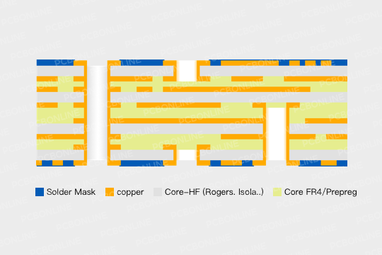
The Basic Structure of High Frequency PCB
The most basic high-frequency PCB has 4 layers and consists of the RF system and the digital circuit.
- The upper layer is the RF system. It consists of a high-frequency circuit and two embedded PCB antennas.
- The second layer is the ground layer. It supplies power to the circuit and also shields the signal radiation and coupling.
- The third layer is the power layer, which supplies power to the circuit and also shields the signal radiation and coupling.
Features of HF PCB
Reduced Moisture Rate
When it comes to moisture, a small amount can distort a high-frequency board’s electrical performance. Interestingly, materials like the PTFE have a moisture rating as low as 2% compared to the traditional FR-4.
Controlled Impedance
The boards contain materials that hold their Dk tolerance at +/-2% or more. That means it’s quite useful for circuits that require tight, controlled impedance..
Dimensional Stability
High-frequency PCBs have thermoset hydrocarbon materials. These materials promote mechanical stability.
Excellent Thermal Management
High frequency PCBs tend to produce a lot of heat during operation. So, with materials like polyimides, you can rest assured that you’ll get robust thermal properties. Plus, you can use them in harsh environments as well.
Excellent Signal Performance
Thanks to its PTFE materials, there’s a low dissipation factor. And it also means that it decreases signal loss.
Applications for HF PCB
High-frequency PCBs work in the way of Radars, and a high-frequency PCB is the core component in a radar application. These also relate to the RF and microwave PCB.
- Radar scopes
- Transmitters
- Receivers
- Antennas
- Power amplifiers
- Low noise amplifiers
- Filters
- Mobile telecom products
- Automobile anti-collision system
Three Main Types of High-Frequency PCBs
RF 6-24GHz PCBs
This type of high-frequency PCB transmits and receives 6 to 24GHz RF signals. RF 6-24GHz PCBs locate objects within 30 meters.
RF 77GHz PCBs
This type of high-frequency PCB transmits and receives 77GHz RF signals. RF 77GHz PCBs can locate objects at a long distance. The signal wavelength that RF 77GHz PCBs generate is two-thirds shorter than RF 6-24GHz PCBs’.
Antenna-embedded PCBs
This type of PCBs have small conductor width, conductor spacing, conductor tolerances, and rounded corners. The RF performance is improved, and the power consumption is reduced.

State-of-the-art HF Manufacturing
Highleap committed to helping customers get the highest quality HF PCBs manufacturing and services at competitive prices.Please feel free to contact us.
Material for High Frequency PCB
Selecting the appropriate material for high-frequency PCBs is crucial for achieving peak performance. Here, we will explore essential factors to consider when choosing high-frequency PCB materials.
Dielectric constant(DK)
The dielectric constant (Dk) represents the relationship between a material’s permittivity and that of free space. It influences the capacitance between conductors and impacts signal propagation speed. Higher Dk values lead to lower characteristic impedance, while lower Dk values result in higher characteristic impedance.
Glass transition temperature
Glass transition temperature (Tg) is a critical parameter as it marks the point at which a material transforms from a rigid state to a more flexible one. This transition significantly impacts the material’s mechanical properties and electrical performance.
Loss tangent
Loss tangent (tan δ) refers to the energy lost as heat due to internal friction within a material. For high-frequency applications, materials with low loss tangents are favored, as they experience minimal signal attenuation, ensuring better performance.
Moisture absorption rate
Moisture absorption rate gauges the material’s ability to absorb water under humid conditions. Excessive moisture can adversely impact the electrical properties of high-frequency PCB materials, causing signal degradation.
Thermal expansion coefficient
The thermal expansion coefficient (CTE) indicates how a material expands or contracts with temperature changes. Materials with low CTE values are beneficial as they reduce stress and distortion resulting from temperature fluctuations.
Cost
Lastly, cost plays a crucial role in the selection of high-frequency PCB materials. While PTFE-based materials offer excellent electrical properties, they tend to be more expensive than FR-4. Similarly, RF Polyurethane materials come at a higher cost compared to FR-4 but offer enhanced performance at higher frequencies.
Rogers RO4003C
Rogers RO4350B
RT/duriod 5870
RT/duroid 5880
Rogers RO3003
Rogers RO3006
Rogers RO3010
isola IS620
AGC Taconic RF-35
AGC Taconic TLX
AGC Taconic TLC
ARLON 85N
Dk(@10GHz)
Df(@10GHz)
”Tg(°C)
Td(°C)
Z CTE(ppm/°C)
Surface Resistivity (MΩ)
Thermal Conductivity (W/m·K)
Peel Strength (N/mm)
Discuss Your HF PCB Project!
Contact us directly to explore these options further and determine the best solutions for your HF PCB needs. Our team at Highleap is ready to assist you in achieving optimal results for your project.
HF PCB Design and Layout Guidelines
1. Fewer vias in your connection
Reduce vias in your connections to minimize distribution capacitance, . Fewer vias lead to increased speed and reduce the risk of data errors.
2.Make a high-frequency lead longer
In this step, the science is that the signal line’s routing length is directly proportional to the radiation intensity. With that in mind, it means that when the high-frequency lead is longer, you’ll find it easy to couple its parts.
3.Reduce the bend
Minimize pin bend in high-frequency boards. Use full straight lines for wiring or 45-degree arc breaks to improve copper foil bonding strength in low-frequency circuits. However, this step isn’t needed for high-frequency circuits to reduce outer emissions.
4.Reduce the crosstalk
Don’t take the crosstalk from the signal line for granted. The crosstalk occurs between signal lines that lack a direct connection. So, it’s best to reduce the crosstalk that occurs in high-frequency signals.
5.Copper Foil Finish for High Frequencies
Higher frequencies cause signals to flow through tracks, producing current. The current density shifts to the outer surface instead of the center, leading to increased copper surface roughness during production. Consequently, signal losses occur at high frequencies.
6. Try not to have loops
Try not to have loops when you’re wiring the HF board. If they occur, make them extremely small.
7.Solder Mask at High Frequencies
Soldermask has a high dissipation factor. So, when you apply it on traces with high frequency, it boosts the circuit’s dielectric loss.
Controlled Impedance
The design of controlled impedance transmission lines is very important in high frequency PCBs, which is for the purpose of avoiding any signal loss. Learn more about Highleap Electronic impedance control services.
There are two common approaches to set controlled impedance transmission lines known as Microstrip and Stripline.
Microstrip
Microstrip is the existence of the trace on the outer layers that come with a ground plane below. The impedance calculation of a microstrip is a little bit tricky and complex though and depends on various factors including relative permittivity of the high frequency PCB base material, thickness and width of the trace and its height above the plane. In order to achieve better result, ground plane must be closer to the outer layers.
Stripline
Stripline is another addition to control impedance which is quite identical to microstrip with one exception, which comes with an extra ground plane on the top of the trace. In this impedance calculation mode, trace must be placed between the layers of two planes. Stripline is better as compared to microstrip because it has an ability to contain EMI radiation within the two planes.
Choose Highleap as Your PCB Manufacturer

Full Expertise
We have rich experience in all kinds of PCB manufacturing and assembly.From component procurement to product delivery, we can complete every step with high quality.

Strong Supplier Network
With 10 years of experience in the PCB industry, Highleap owns a supplier network that provides us with reliable access to get high-quality components at competitive prices.

Strict Quality Control
At each process, we strictly control the quality by implementing a variety of testing and inspections to ensure that each PCBA reaches the highest quality standard.
Take a Quick Quote
Discover how our expertise can help with your next PCB project.
