
Professional PCB Design Services
Highleap Electronics offers complete PCB design services covering schematic diagram, PCB layout, DRC, DFM, DFA, DFT, and impedance control—ensuring manufacturable, testable, and high-performance boards.

From Concept to Prototype
One-Stop PCB Design Solutions
Struggling with complex PCB design challenges, tight deadlines, or costly design iterations? Highleap Electronics’ comprehensive PCB Design Services eliminate the guesswork and accelerate your product development cycle. Whether you’re a startup racing to prototype or an enterprise scaling production, our expert-level PCB design services bridge the critical gap between engineering theory and manufacturing reality.
Meet a variety of needs
PCB Design Services Portfolio

Schematic Diagram
Whatever you need the service of convert PCB to schematic diagram or from concept to schematic diagram, our engineers are happy to help.

DFA
Properly adhering to PCB DFA guidelines can lead to reduced production costs, shorter time-to-market, and enhanced product reliability.

PCB Layout
From a schematic diagram to PCB layout, we can provide professional PCB layout services that ensure optimal performance.
DFT
PCB DFT services optimize designs for easier, more efficient testing and quality verification during manufacturing.
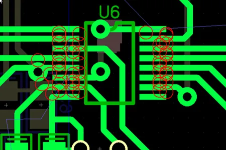
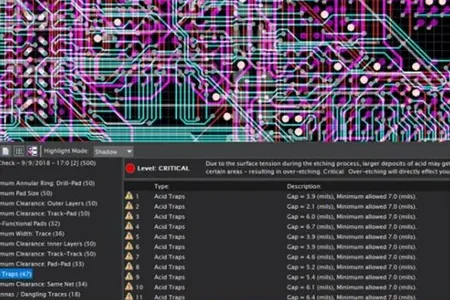
DRC
The fusion of PCB Design Rule Check and the PCB layout process has ushered in a new era of efficiency and precision.

Impedance Control
Highleap controls impedance with precise routing and matching components to ensure signal integrity.
DFM
We offer a valuable Free DFM Check. This service bridges the knowledge gap between PCB designers and manufacturing requirements.
Stages of PCB Design Services
Define Scope
Define functionality, specifications, and constraints clearly.
Schematic Design
Create the schematic diagram and logic connections.
Part Selection
Choose components based on performance, cost, and availability.
PCB Layout
Place components and plan routing strategically.
Routing
Auto/manual routing to complete signal paths.
Design Rule Check
Run DRC to verify layout against rules and standards.
Partner with Highleap Electronic
Why Choose US
Advanced Multilayer PCBs
Capable of manufacturing 1–60 layer PCBs with high precision.
Senior Engineering Team
Engineering team with 10+ years of PCB design & production experience.
Strict IP & File Confidentiality
Free Prototype Testing
Start Your PCB Project!
Highleap specializes in the design and manufacturing of complex PCBs, with over 10 years of experience. Our expertise allows us to tackle high-difficulty projects with precision and reliability. Send your request now!
PCB Design Services
Comprehensive Solutions for Custom PCB Needs
At Highleap Electronics, our PCB design services cover a wide spectrum of industries and technical requirements. From simple FR4 PCB design to complex multilayer PCB design, we deliver high-quality custom PCB design services tailored to your project. Whether you need flexible PCB design, rigid-flex PCB design, high-frequency PCB design, or metal-core PCB design, our expert engineers ensure optimized performance, manufacturability, and cost-effectiveness.

Diverse PCB Types & PCB Materials in Design Services
Our PCB design services include expertise with various PCB types and materials, suited for different applications:
2. Flexible PCB Design Services: Support for dynamic, bendable circuits in wearable tech, medical devices, and compact electronics. Our flexible PCB design services help reduce space and weight in products like foldable smartphones, fitness trackers, and hearing aids, where repeated bending is essential.
3. Semi-Rigid PCB Design Services: Semi-rigid PCBs offer a hybrid solution that blends the flexibility of flex circuits with the structural support of rigid boards. Ideal for semi-rigid circuit board applications in automotive, aerospace, and industrial electronics, these designs provide controlled flexing while ensuring mechanical durability in constrained spaces.
4. Rigid-Flex PCB Design Services: Integration of rigid and flexible substrates in one board, perfect for space-constrained and durable device designs. Rigid-flex circuit design is ideal for compact devices such as digital cameras and medical implants, offering reduced wiring and improved reliability under stress.
5. Metal-Core PCB Design Services: Thermal management for LED lighting, automotive, and power electronics requiring heat dissipation. Our metal core PCB design solutions use aluminum or copper substrates to enhance heat dissipation in high-power LEDs and motor driver circuits.
6. Heavy Copper PCB Design Services: For power electronics and industrial systems demanding high current capacity and thermal reliability. Heavy copper PCB layout supports high current loads, commonly used in power converters, solar inverters, and industrial control systems.
7. Power PCB Design Services: Power PCB design focuses on handling high current and voltage with stability and efficiency. These boards incorporate reinforced copper planes and optimized thermal management, making them essential for power supply units, motor controllers, and energy storage systems operating under demanding electrical conditions.
8. High-Frequency and RF PCB Design Services: Minimizing signal loss and ensuring signal integrity for communication and microwave circuits. Our RF PCB design service includes impedance control and low-loss materials, ideal for 5G modules, satellite receivers, and radar applications.
9. Ceramic PCB Design Services: High thermal conductivity and insulation for harsh environment electronics. Ceramic PCB design is preferred for high-temperature and high-voltage applications like laser systems, automotive sensors, and RF amplifiers.
10. High-Speed PCB Design Services: High-speed PCB design prioritizes signal integrity for fast and accurate data transmission. Using controlled impedance, low-loss substrates, and precise trace routing, these boards are essential for high-speed data systems such as routers, servers, telecom infrastructure, and advanced computing devices.
PCB Design and Engineering Details
While the design flowchart outlines the major steps in PCB development, there are many critical engineering details that happen behind the scenes to ensure quality, performance, and manufacturability. At Highleap, our engineering process adds depth to each stage—especially in areas like layout precision, signal control, and rule validation—that are essential for professional-grade circuit design.

1. Schematic Design & Requirements Analysis
We begin by thoroughly analyzing your project’s electrical and functional requirements. Our engineering team then creates a detailed schematic, defining logical connections, power distribution, and selecting components that align with performance and sourcing goals.
2. Component Placement & Layout Optimization
Strategic component placement is key to signal integrity, thermal performance, and manufacturability. We consider trace lengths, return paths, heat dissipation, and 3D form factor constraints to deliver optimal printed circuit board layout design.
3. Signal Routing & Pattern Engineering
Our routing process focuses on high-speed and high-density trace optimization. We implement controlled impedance, matched differential pairs, and low-noise layout principles—supporting applications such as RF circuits, power electronics, and HDI PCBs.
4. Design Rule Check (DRC) & Electrical Validation
Beyond standard layout, we perform comprehensive DRC to catch clearance violations, via misplacements, and trace width issues. Electrical rule checks validate the schematic-to-layout integrity, preventing design-stage errors from entering production.
5. Manufacturing Documentation & Output
We generate precise PCB artwork and complete documentation packages—including Gerber files, BOMs, pick-and-place files, and fabrication notes. These outputs ensure consistency and quality throughout board fabrication and assembly stages.
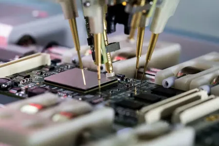
Prototyping, Fabrication, and Assembly Services
1. PCB Prototyping Services
We deliver fast, accurate PCB prototyping for rigid, flexible, and HDI boards. Our quick-turn prototypes help verify layout and electrical performance early, reducing risks and speeding up development.
2. Custom PCB Manufacturing
We offer tailored custom PCBs, including unique shapes, advanced materials (aluminum, ceramic, high-frequency laminates), and multilayer stackups. Our designs are optimized for your electrical, thermal, and mechanical requirements.
3. PCB Fabrication and Assembly Services
Our comprehensive fabrication and assembly services cover sourcing, bare board production, SMT assembly, and testing. We handle metal core, ceramic, and HDI PCBs with leaded or lead-free options, ensuring quality and timely delivery.

Advanced Signal Integrity and Power Integrity Management
Signal Integrity Analysis in High Frequency PCB Designs
Ensuring signal integrity is critical for achieving reliable and high-performance PCB designs. At Highleap, our process incorporates comprehensive signal integrity analysis to address key factors such as impedance matching, noise reduction, and reflection minimization. This is particularly essential for high-frequency (HF) PCBs and RF PCBs, where signal clarity and consistency are paramount for optimal communication and data transmission. Our design focus ensures that signal paths remain stable and interference-free, enhancing overall functionality and efficiency.
Power Integrity Optimization in Power and Heavy Copper PCBs
Power integrity is equally crucial, especially for designs involving substantial electrical loads. We meticulously design robust power distribution networks (PDNs) and implement effective decoupling strategies to maintain stable voltages and currents. This approach is particularly significant for power PCBs and heavy copper PCBs, which often handle high-current scenarios and complex power management requirements. By creating well-structured PDNs, we reduce voltage fluctuations and ensure consistent power delivery across all critical components, ultimately improving the reliability and longevity of the circuit.
Future-Ready and Specialized PCB Solutions
In addition, our high-speed PCB design expertise supports growing requirements in telecommunications and networking, where signal integrity and rapid data transmission are critical. By integrating controlled impedance and optimized trace geometry, we ensure stable high-frequency performance across complex multilayer boards.
Tailored PCB Solutions for Specialized Applications
Highleap provides custom PCB design services tailored to a wide range of industries. Whether you need:
- Flexible PCBs for wearable electronics and medical sensors
- High-power PCBs for power electronics and energy storage systems
- RF and high-frequency PCBs for wireless communication or radar systems
—we collaborate with clients to create optimized, application-specific designs. Our engineering team balances performance, reliability, and cost-efficiency, ensuring that each circuit board meets both functional and commercial requirements. From concept to manufacturing, our end-to-end support helps clients bring innovative products to market faster and more confidently.
FAQ
1. What types of PCB design services does Highleap Electronics provide?
Highleap Electronics offers end-to-end PCB design services covering schematic capture, layout, signal integrity simulation, and DFM optimization. We support a wide range of board types including FR4 PCBs, flexible circuits, rigid-flex boards, and HDI PCBs. Whether you’re working on single-layer or multilayer PCBs, our engineers can tailor the design to your specific electrical, thermal, and mechanical requirements.
2. How does Highleap ensure the quality of PCB design before manufacturing?
Before fabrication, our team performs detailed DFM (Design for Manufacturability) and DFT (Design for Testability) checks, impedance control validation, and design rule checks (DRC). We also offer prototype testing services to verify electrical performance and manufacturability. These design verification steps help reduce risk and ensure first-time-right production.
3. Can you help with both PCB design and manufacturing in one stop?
Yes. Highleap provides full turnkey solutions that integrate PCB design and manufacturing services. From concept to final production, we streamline the process to reduce lead times, ensure design accuracy, and simplify vendor management. This one-stop approach is ideal for startups, OEMs, and teams working under tight deadlines.
4. What industries do your PCB design solutions support?
Our PCB design services support a broad range of industries including medical electronics, industrial control systems, automotive electronics, LED lighting, and consumer electronics. We can comply with various standards such as ISO13485 and IATF16949, making us a reliable partner for both standard and specialized PCB projects.
Get a Quick Quote!
Highleap specializes in the design and manufacturing of complex PCBs, with over 10 years of experience. Our expertise allows us to tackle high-difficulty projects with precision and reliability. Send your request now!