Laser Cut PCB Stencil
Empower Your Electronics Manufacturing! Maximize yield and minimize defects with our premium laser-cut PCB stencils, engineered to deliver peak performance.
What is Laser Cut PCB Stencil?
Laser parameters are optimized to cut complex aperture shapes and allow very fine feature sizes down to 20 μm. Laser cutting enables tight tolerances of ±10 μm for intricate PCB patterns. Advanced motion control guides the laser beam over the stencil surface and sophisticated projection optics precisely align the cut locations. Materials like stainless steel and brass are readily processed.
Laser cut stencils promote consistent solder paste release and printing uniformity due to the smooth aperture walls and edges. Automated in-line inspection validates aperture dimensions. The laser process avoids tool wear issues compared to mechanical milling or chemical etch approaches. Laser cut stencils provide precision and accuracy needed for today’s high density PCB designs, while enabling rapid turnaround and scalability to high production volumes.
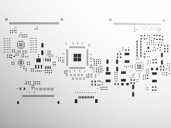
Laser Cut PCB Stencil Category
The laser cutting of PCB templates can be classified based on various factors, including the type of material used, the thickness of the template, and the complexity of the PCB design. Furthermore, depending on the chosen solder paste application method, the steel mesh can be further categorized as framed or frameless.
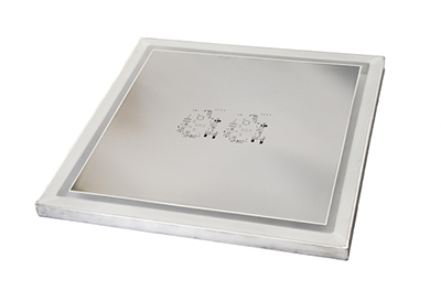
Framed stencils
Framed stencils are securely mounted on a metal frame, providing stability during the solder paste application process. The frame helps ensure precise alignment and consistent pressure during the stencil printing, leading to uniform solder paste deposits on the PCB pads. This stability and support offered by framed stencils contribute to efficient and reliable surface mount assembly, particularly for high-volume production environments.

Frameless stencils
Frameless stencils, utilizing a tensioning system, eliminate the need for metal frames, offering enhanced flexibility in usage and storage. Perfect for smaller production runs and prototyping, they significantly reduce overall cost and space requirements, making them an ideal choice for varying PCB designs or frequent changes, ensuring efficient production workflows and streamlined processes.
By carefully selecting the appropriate type of laser-cut PCB template, manufacturers can achieve accurate and reliable solder paste deposition, leading to high-quality PCB assembly and optimal performance of electronic devices. If you have any specific requirements or questions, please feel free to contact the Highleap team for assistance.
Laser-cut PCB templates come in various types, each offering unique advantages tailored to specific design and assembly requirements. In addition to the frameless and framed laser-cut PCB templates, other common types include step-up templates for varying component heights, nano-coated templates for improved solder release, and electroformed templates with independent aperture count.
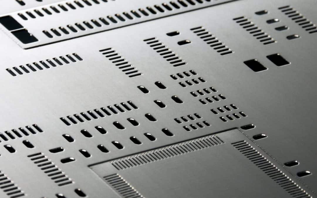
Step stencils
These templates have varying thickness in different sections to accommodate components of different heights, ensuring precise deposition of solder paste in designated areas of the PCB.
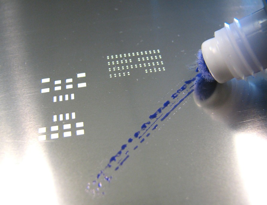
Nano-coated templates
These templates undergo a thin nano-coating process to improve solder release and reduce bridging, providing better printing performance for challenging PCB designs.
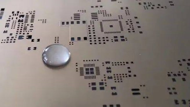
electroforming or E-FAB template
Produced using an additive process involving electroplated nickel. Although this method may involve higher initial costs, it has the advantage of not being dependent on the number of apertures. However, its longer processing time is considered a disadvantage.
Laser Cut PCB Stencil Production Steps
Making a PCB stencil involves several precise steps to ensure accurate solder paste application during the PCB assembly process. Here is a professional and detailed explanation of how a PCB stencil is made:
PCB Design
The first step is to create the PCB design using computer-aided design (CAD) software. The PCB layout includes the positions of components and their corresponding solder pads.
Stencil Design
Based on the PCB design, a stencil design file is generated. This file contains information about the size, shape, and position of the apertures on the stencil, which align with the solder pads on the PCB.
Material Selection
The material for the stencil is chosen based on factors such as the complexity of the PCB design, the required thickness, and the desired performance characteristics. Common materials include stainless steel and brass.
Laser Cutting
Laser micromachining is used to cut the stencil material and create precise apertures. The laser parameters, such as power, pulse rate, and focal spot size, are carefully optimized to achieve accurate and smooth cuts with minimal thermal effects.
Inspection
After laser cutting, the stencil undergoes rigorous inspection to ensure the apertures’ dimensions conform to the original design specifications. Advanced in-process inspection and metrology techniques, like scanning electron microscopy and automated optical inspection, may be employed to verify the stencil’s precision.
Nano Coating (Optional)
Some stencils may undergo a nano coating process to improve solder paste release and reduce bridging during printing. This optional treatment enhances the stencil’s printing performance, especially in challenging PCB designs with fine-pitch components.
Framing (Optional)
Depending on the stencil type, it may be framed or frameless. Framed stencils are mounted on a metal frame to provide stability during solder paste application, ensuring consistent alignment and tensioning. Frameless stencils are held in place using a tensioning system, offering flexibility and ease of use.
Packaging and Delivery
The final step involves packaging the stencil to protect it during shipping and storage. Stencils are carefully packaged to prevent damage during transit and delivered to the PCB assembly facility.
The precision and accuracy achieved during the PCB stencil manufacturing process are critical for successful surface mount assembly. Laser cut PCB stencils enable consistent and reliable solder paste deposition, ensuring the high-quality assembly of electronic components on the PCB. Properly manufactured stencils play a vital role in optimizing production efficiency and product reliability in today’s electronics manufacturing industry.
PCB Stencil Design Tips and Considerations
Adhering to these PCB stencil design tips and considerations enables engineers to optimize solder paste deposition, reduce defects, and ensure a successful surface mount assembly process, ultimately leading to high-quality PCB assemblies with reliable solder joints. By carefully implementing these design strategies, engineers can enhance the overall performance and reliability of electronic devices, meeting the demands of modern technology and providing a competitive edge in the industry.
Aperture Size and Shape
Carefully determine the aperture size and shape to match the corresponding solder pads on the PCB. The aperture size should be slightly larger than the pad size to ensure proper solder paste deposition while minimizing solder bridging. Use precise aperture shapes for fine-pitch components, and consider round or rectangular shapes for optimal paste release.
Aspect Ratio and Stencil Thickness
Pay attention to the aspect ratio of the apertures (the width-to-thickness ratio). High aspect ratios can lead to stencil clogging, while low ratios may result in insufficient paste deposition. Select the appropriate stencil thickness based on the PCB design and assembly requirements. Standard thickness stencils are suitable for most applications, but step stencils are essential for varying component heights.
Framed vs. Frameless Stencils
Choose between framed and frameless stencils depending on the assembly process and equipment used. Framed stencils provide stability during printing and are ideal for high-volume production. On the other hand, frameless stencils offer flexibility and are suitable for small volume production or prototype testing. The type of stencil can have a significant impact on the solder paste printing quality and overall assembly process.
Choose Highleap’s Laser-Cut PCB Stencils

Full Expertise
Highleap boasts years of experience and technical proficiency in the PCB industry. Our team is well-versed in the latest laser-cutting technologies and manufacturing processes, enabling us to deliver high-quality laser-cut PCB stencils tailored to diverse design and assembly requirements.

Robust Supplier Network
We collaborate with outstanding suppliers, ensuring access to high-quality stencil materials and advanced laser-cutting equipment. This partnership ensures that we can provide laser-cut PCB stencils at optimal cost and efficiency while guaranteeing timely delivery.

Strict Quality Control
At Highleap, quality is our utmost commitment. We implement stringent quality control measures, including thorough inspections and validation through the entire process, to ensure the precision and reliability of each laser-cut PCB stencil. This dedication to quality assurance makes us a trusted partner.
