Advanced HDI PCB Manufacturer
Experience professional high-density interconnect PCB manufacturing with turnaround times as short as 5-15 days!
What is HDI PCB
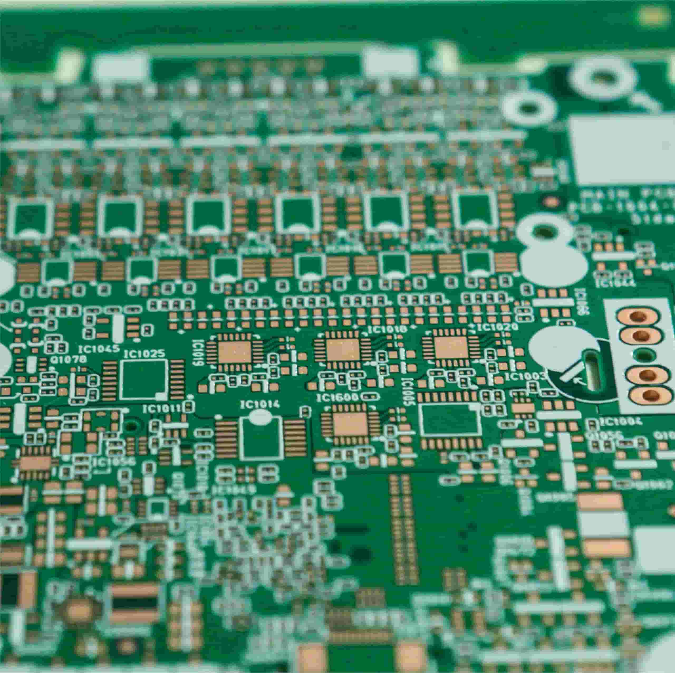
HDI PCB, which stands for high-density interconnect printed circuit board. HDI PCBs are designed with thin lines, close spaces, and dense wiring, allowing for faster and more reliable signal transmission.
By incorporating innovative features such as blind and buried vias, laser-drilled microvias, sequential lamination, and via in-pads, these boards have pushed the boundaries of what is possible in terms of size reduction and high-speed performance.
Types of HDI PCB
HDI PCBs are available in various types, here are some common types of HDI PCBs:
1+N+1
In this stackup, “1” represents a core layer with copper on both sides, and “N” indicates the number of additional copper layers added on top of the core layer.
These stackups are well-suited for devices like high-end smartphones, tablets, laptops, and other advanced consumer electronics.

HDI PCB 1+N+1 construction

2+N+2
With the 2-N-2 stackup, there are two core layers sandwiched between multiple additional copper layers.
These stackups are well-suited for high-performance computing, telecommunications equipment, medical devices, and other advanced electronic applications.
3+N+3
These stackups are particularly suitable for modern smartphones, tablets, wearable devices, high-speed communication equipment, and other compact electronic devices .
However, it also requires precise manufacturing processes and advanced PCB fabrication capabilities to ensure reliable and high-quality boards.

HDI PCB – Every Layer Interconnection
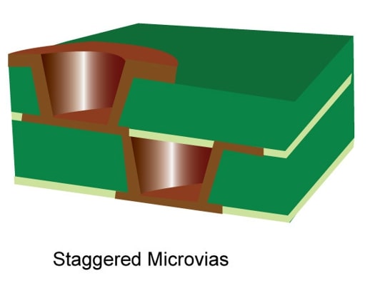
Staggered via HDI PCB
In the staggered via HDI PCB, the microvias are staggered between different layers, providing more flexibility and space for routing traces and connecting components.
By using staggered vias, designers can optimize the signal paths and reduce signal losses, ensuring better performance and reliability of the electronic device.
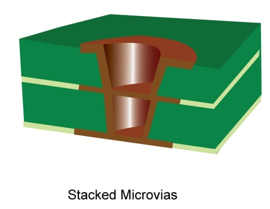
Stacked via HDI PCB
In the stacked via design , microvias are stacked on top of each other to create vertical connections between different layers of the PCB.
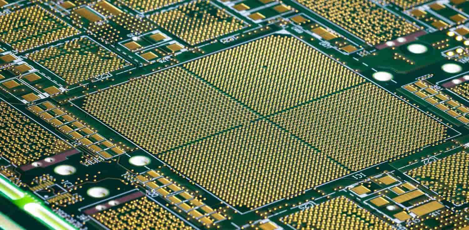
The right HDI stack-up reduce your costs!
HDI PCB costs can be reduced when your stack-up is properly planned out. Engineers at Highleap Electronic can help you efficiently prototype and manufacture your printed circuit boards. Or click to learn more about stack-up of HDI PCB.
Advantages of HDI PCB
If you choose to design and produce hdi pcb, because of its characteristics, you can enjoy the following characteristics:
Reduction in heat transfer
HDI PCBs offer the advantage of reduced heat transfer. With a compact design, heat travels shorter distances within the PCB, allowing for efficient heat dissipation. Additionally, the high thermal expansion capability of printed circuit boards contributes to a longer lifespan.
Manages thermal conductivity
By strategically placing via-in-pad and blind vias components together, this configuration reduces transmission distances, resulting in shorter transmission times and reduced crossing delays. As a result, your PCBs will exhibit strong signal performance.
Smaller form factors
By optimizing the design , you can reduce the number of layers required. This results in a smaller PCB footprint, while still maintaining the necessary vias for performance. Additionally, the reduced layer count contributes to a cleaner and less visually cluttered appearance of the PCB.
Less power usage
HDI PCBs offer the advantage of reduced power consumption, resulting in extended battery life. By utilizing vias instead of through holes, high-density PCBs efficiently reduce power usage, making them an ideal choice for maximizing battery performance.
Incorporating components
Because the PCB’s space can be minimized for the components, it is possible to integrate whatever details you desire on the board,and you can increase or decrease the number of layers.
Applications for HDI PCB
Consumer Electronics
These include smartphones, computers, home appliances, laptops, entertainment systems, and recording devices.
Industrial Applications
HDI PCBs are usually seen as the standard in highly-powered industry. HDI PCBs with thick copper to ensure high current and fast battery charges .
Aerospace Applications
The precision and durability offered by HDI PCB ensures the majority of aeronautical equipment the harsh environments .
Medical Equipment
Some medical devices prove the importance of HDI PCB,such as scientific instruments, control systems, heart peacemakers, scanners, and monitors.
Automotive Applications
The application of HDI PCBs can be done to sensor applications usually found in automotives.
Lighting Applications
The HDI PCB is also very useful in different LED applications.These components are close; this means that there is a reduced loss of energy to the surrounding. This ensures maximum output.
Start Your PCB Project!
Highleap has extensive experience in manufacturing HDI PCBs for customers in different industries such as medical, automotive, and electronics.
We have the ability to handle all HDI PCBs projects with unmatched accuracy and high quality within your budget.
Material Selection for HDI PCB
Selecting the right dielectric material or resin is important for HDl performance. The following properties are critical:
Decomposition Temperature (Td)
The HDI PCB material should have a Td that is well above the temperature range of its application. The solder temperatures during HDI PCB assembly are in the 250 ℃ to 300 ℃ range, so make sure that the material’s Td is higher than this range.
Dielectric Constant (Dk)
For HDI PCBs, it is preferable to use substrate materials with a low DK value. The lower the DK value, the better the signal integrity and impedance control, particularly at higher frequencies. Low DK materials minimize signal loss, crosstalk, and other electrical issues, ensuring reliable performance for high-speed digital and RF signals.
Glass Transition Temperature (Tg)
When producing an HDI PCB, material with a high Tg is typically chosen.FR4 with a Tg of 170°C or higher is commonly used for these PCBs, as it provides excellent thermal and mechanical properties.
Loss tangent
The power loss of a signal as it passes through a transmission line on a dielectric material.
Coefficient of Thermal Expansion (CTE)
This sudden expansion and contraction of the circuit can have devastating consequences on components, especially large silicon chip packages. Excessive thermal cycling result in the failure of solder joints because the circuit expands at a faster rate than the silicon chip is rated to tolerate. Furthermore, this will result in shear forces that create micro tears over time.
Common Materials for HDI PCBs
We have sufficient inventory of different types of HDI PCB materials and long-term cooperation with excellent suppliers to escort your HDI PCB plan.
Normal Speed and Loss
Normal speed and loss materials are best suited to digital devices that are limited to a few GHz. A popular example of such a material is Isola 370HR.
Medium Speed and Medium Loss
Medium speed materials are best suited to applications that are limited to 10 Ghz but not any higher. The Nelco N7000-2 is a popular example from this category of materials.
High Speed, Low Loss
These materials have the advantages of low dielectric loss and little electrical noise. These high performance materials have a Tg of nearly 180°C.A popular example of high speed, low loss material is Isola’s I-Speed.
Very High Speed, Very Low Loss
Very High Speed, Very Low Loss materials suit to applications that go up to 100 Ghz and higher. The Isola Tachyon 100G is a popular material that belongs to this category.
HDI PCB Manufacturing Technology
The difficulty in HDI PCB manufacturing is microvias, which are made through metallization and thin wires.
Microvia manufacturing
Microvia manufacturing has always been the core issue of HDI PCB manufacturing. There are two main drilling methods:
1.Mechanical drilling, which for ordinary through hole drilling is always the best choice for its high efficiency and low cost. With the development of machining capabilities, its application in microvias is also constantly developing.
2.Laser drilling, of which there are two types: photothermal ablation and photochemical ablation. The former refers to a process by which the operating material is heated to melt and evaporate through the formed through hole after the high-energy laser is absorbed. The latter refers to the result of high-energy photons and lasers exceeding 400nm in the ultraviolet region.
Through metallization
The biggest challenge of through-hole metallization is that it is difficult to achieve uniform plating. For the deep-hole electroplating technology of microvias, in addition to the use of an electroplating solution with high dispersibility, the plating solution on the electroplating device should be upgraded in time. This can be done through strong mechanical stirring or vibration, ultrasonic stirring, and horizontal spraying. In addition, the humidity of the through-hole wall must be increased before plating.
In addition to process improvements, HDIs’ through-hole metallization method has also seen major technological improvements: these include chemical plating additive technology, direct electroplating technology, etc.
Tiny circuit
The realization of thin lines includes traditional image transmission and direct laser imaging. Traditional image transfer is the same as the process of forming lines by ordinary chemical etching.
For direct laser imaging, the image is formed directly on the photosensitive film by laser. The ultraviolet (UV) lamp is used for operation, so that the liquid anticorrosion solution can meet the requirements of high resolution and simple operation.CAD/CAM can be directly connected to shorten the manufacturing cycle and make it suitable for limited and multiple production.
HDI PCB Manufacturing Capabilities
- Back drilling – A method of disconnecting part of the plated through hole from other layers inside.
- Controlled depth drilling/milling
- Buried capacitance – This technology can increase the performance of printed circuit boards through improved signal integrity. This process incorporates a very thin dielectric layer that provides distributive decoupling capacitance.
- Hole tolerances – With our advanced technology drilling equipment, we’re able to hold very tight hole tolerances and hole locations. This is importance because these holes have multiple functions, including through-hole connector insulation
Choose Highleap as Your PCB Manufacturer

Full Expertise
We have rich experience in all kinds of PCB manufacturing and assembly.From component procurement to product delivery, we can complete every step with high quality.

Strong Supplier Network
With 10 years of experience in the PCB industry, Highleap owns a supplier network that provides us with reliable access to get high-quality components at competitive prices.

Strict Quality Control
At each process, we strictly control the quality by implementing a variety of testing and inspections to ensure that each PCBA reaches the highest quality standard.
Take a Quick Quote
Discover how our expertise can help with your next PCB project.
