PCB Equipment and Process
With Highleap’s PCB equipment, every process is meticulously controlled, guaranteeing impeccable product quality.
Manufacturing PCB Process
The concept of a “standard” printed circuit board (PCB) is illusory, as each individual PCB serves a distinctive purpose tailored meticulously to a specific product. Consequently, the fabrication of a PCB engenders a labyrinthine process characterized by a multitude of intricate stages. This comprehensive overview encapsulates the pivotal junctures intrinsic to the creation of a multifaceted multilayer PCB.
Upon engaging Highleap as your provider of choice for PCB procurement, you are not merely securing a product; rather, you are making an investment in an enduring hallmark of quality. This assurance is underpinned by an exacting product specification and a rigorously enforced quality control regimen that far surpasses prevailing industry benchmarks, thereby furnishing an unequivocal substantiation of performance. The ensuing explication of the production sequence affords a discerning insight into the unparalleled attributes that define the Highleap process, which distinctly transcends the established norms of the industry.
For more information on PCB fabrication processes, please consult our engineers at Highleap.The following only shows some PCB equipment.For a complete equipment list or further information, please don’t hesitate to contact us. Below is an example overview of a multilayer PCB production:
1. Engineering Document Production
In the realm of PCB manufacturing, CAM (Computer-Aided Manufacturing) emerges as a pivotal technology, orchestrating the transformation of circuit board designs into indispensable data and procedural files requisite for tangible fabrication. At its core, CAM serves as the conduit for transmuting circuit board design data into manufacturing data, primed for integration within imaging procedures and drilling protocols.
Within the PCB manufacturing spectrum, CAM undertakes a multifaceted role, encompassing:Gerber data conversion、Process analysis、Process optimization、Process setup、Navigation files output、Process verification、Data management;In summary, CAM software serves as a bridge connecting design to manufacturing, enabling smooth data conversion into actual PCB products.
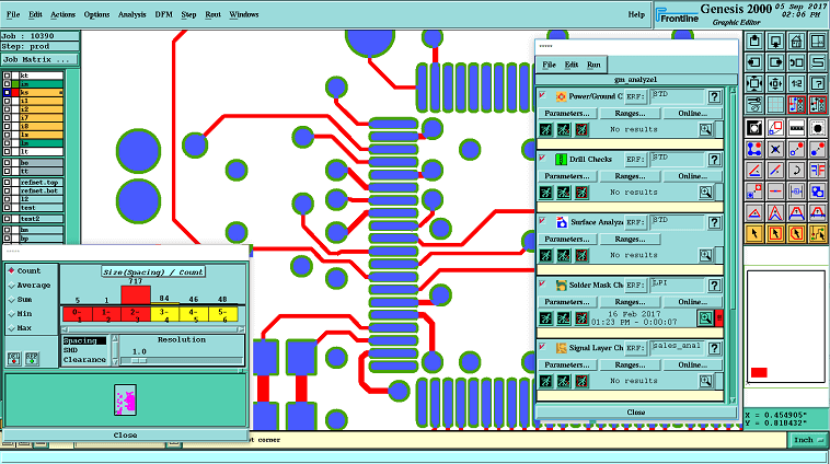
genesis 2000
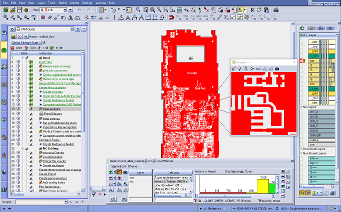
Incam
2. Material Cutting
The initiation of PCB production commences with the utilization of a sizable sheet of material. Recognizing the constraints posed by the prevailing PCB production equipment and manufacturing capabilities, the production facility stipulates specific parameters encompassing both the lower and upper thresholds pertaining to processing dimensions. To ensure adherence to these precise specifications, the initial stages entail meticulous adherence to manufacturing instructions (MI). This mandates the preliminary utilization of an automated cutting machine to accurately segment the raw material, denoted as Copper Clad Laminate (CCL), into dimensions aligning seamlessly with the designated processing size. This preparatory phase is indispensable to the subsequent phases of production, underscoring the precision and methodical approach integral to PCB fabrication.
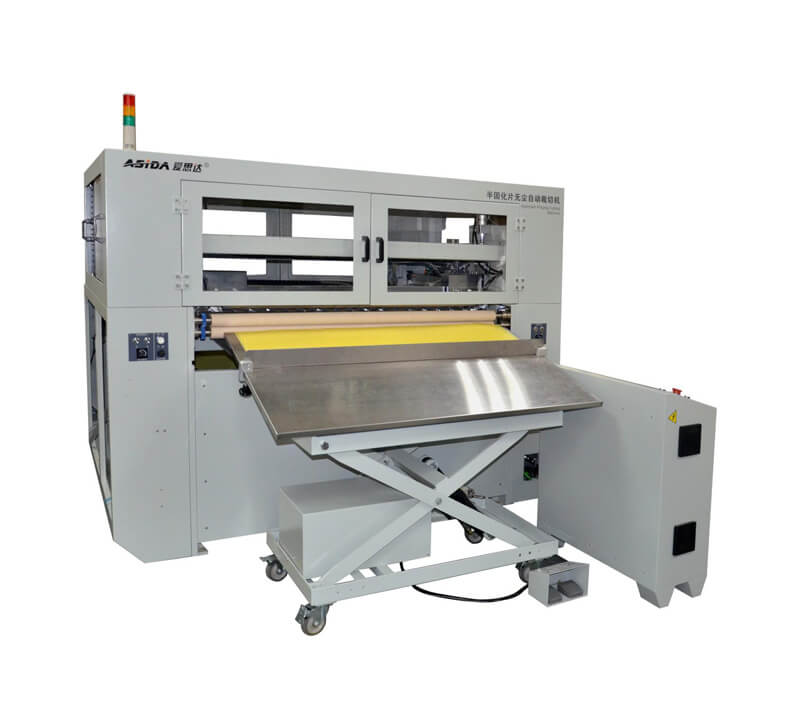
Prepreg Cutting
3. Print inner layers
The circuit pattern is transferred to the board surface using a photomask and UV exposure of the photosensitive dry film laminate. UV light causes polymerization in exposed areas of the dry film. The photolithography process is performed in a clean room environment.
Imaging is the process of converting electronic design data into a format readable by an optical plotter. A photoplotter then uses ultraviolet light to expose a negative image of the circuit pattern directly onto the panel or photomask film.

Auto Roller Coating System
4. Inner layer etching
Inner layer etching, this is a crucial process. The goal here is to precisely remove excess copper from the panel through a well-planned etch process. After completing this critical stage, the residual dry film is carefully removed, leaving a carefully configured copper circuit that perfectly reflects the complexity of the specified design.
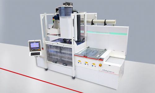
Etch equipment
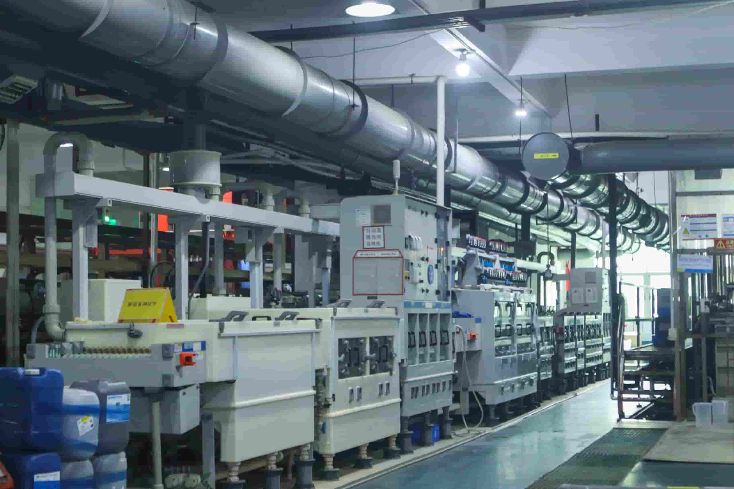
Etching equipment
5. Inner Layer AOI
The Inner Layer Automatic Optical Inspection (AOI) at Highleap is a pivotal quality control point. This intricate process thoroughly compares the circuitry against digital images to ensure design alignment and eliminate imperfections. A comprehensive board scan and inspection by highly trained technicians detects any anomalies. Notably, Highleap upholds a stringent standard – open circuits are not repaired. This commitment exemplifies our dedication to uncompromising quality.
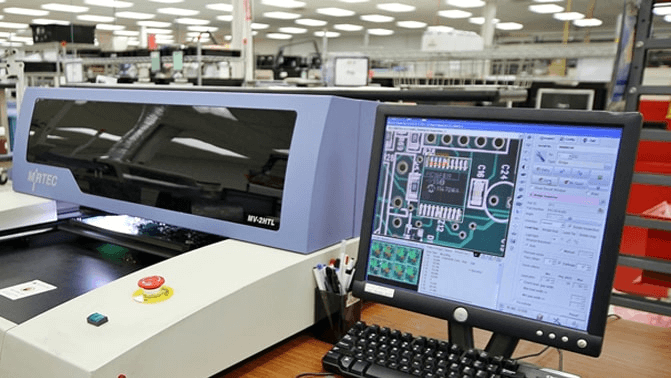
AOI
6. Oxidation
The PCB brown oxide process, also known as PCB brownization or black oxide process, serves the purpose of enhancing the adhesion and solderability of copper surfaces on the circuit board. This process involves the controlled chemical oxidation of the exposed copper, forming a thin layer of brown or black oxide on the copper surface. This oxide layer improves the bonding between the copper and the substrate materials, as well as promotes better wetting during the soldering process. Additionally, the brown oxide layer acts as a protective barrier, safeguarding the copper traces from oxidation and ensuring prolonged shelf life and reliable performance of the PCB.
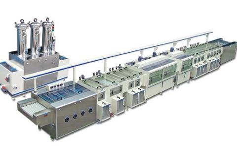
Oxidation system
7. Lay-up and Bond (Lamination)
Inner layers are oxidized then stacked and aligned to form the board structure. Prepreg material separates the layers as an insulator, while copper foils are added to the top and bottom. The lamination process precisely combines heat, pressure, and photoresist to form a cohesive laminate. Layers are heated to 375°F and pressurized from 275-400 psi. After curing at high temperature, pressure is gradually released and the board is cooled in a controlled sequence. This meticulous process creates a sound, high-quality PCB.
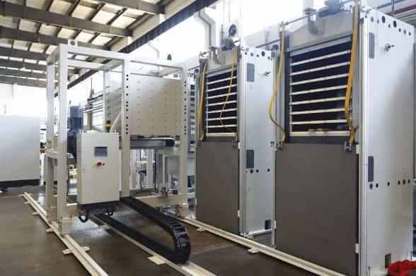
Lamination
8. Drilling the PCB
The PCB drilling process is crucial for creating interconnections between layers. Holes known as vias allow traces and components to connect across multilayer boards, enabling complex circuitry to function. Additionally, holes are drilled for through-hole components and mounting points. Precision drilling is paramount to ensure proper alignment and connectivity in the PCB design.
At Highleap, we utilize numerically controlled drills and advanced software to reliably produce boards with highly accurate holes. Both round holes and rectangular slots are drilled to match the layout precisely. This guarantees design integrity whether for vias, components, or flexibility in placement. Furthermore, we offer metalized slot milling capabilities. This process machines trenches in the copper layers of the PCB and then electroplates the walls of the slot to create conductive paths. Metalized slots serve specialized functions such as RF transmission lines or high current capacity connections. With expertise in precision drilling and metalized milling, Highleap delivers PCBs with superior hole quality and advanced functionality.
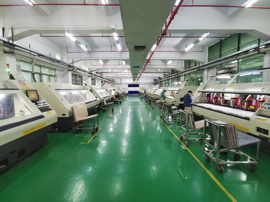
PCB Drilling Machines-PCB equipment
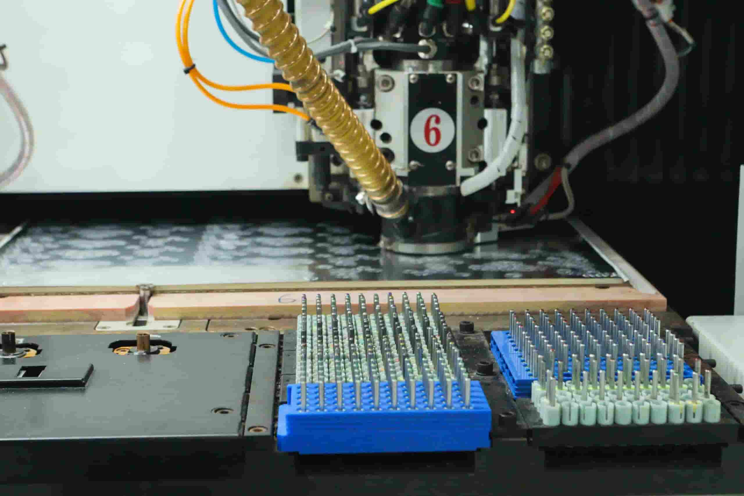
PCB Drilling Machines-PCB equipment
PCB drilling production video-PCB equipment
9. Electroless copper deposition
Electroless copper deposition forms a delicate copper layer on the interior walls of drilled holes, establishing electrical continuity between layers. This precise chemical process requires careful control to ensure a reliable deposit even on non-metallic surfaces. The subsequent through-hole plating envelops the hole walls and board surface with this thin copper coating.
At Highleap, we expertly balance the copper plating thickness between 5-8 microns during panel plating. This follows the initial PTH layer and optimizes the copper for subsequent etching according to exacting track and gap specifications. Our meticulous plating orchestration fulfills the most demanding PCB requirements.
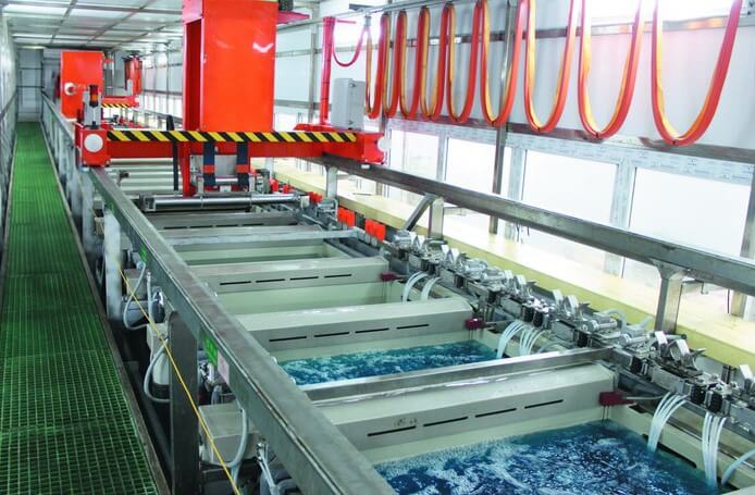
Electroless copper deposition
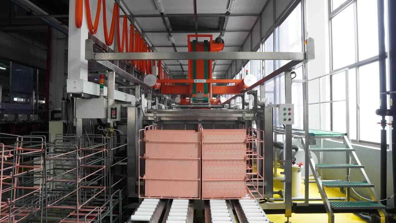
Electroless copper deposition
10. Outer dry film (Image the outer layers)
Outer layer dry film lamination applies a photosensitive coating onto the external copper layers of a PCB before imaging and etching. The dry film photoresist protects the copper during etching to form conductors and traces. First, heat and pressure adhere the dry film. Next, UV exposure through a photomask and developing create a resist pattern. The remaining photoresist shields the copper traces from etching. Finally, the dry film is stripped, leaving only the desired conductor pattern.
At Highleap, we utilize advanced lamination and exposure processes essential for achieving fine line resolutions and tight tolerances. Our expertise in outer layer dry film patterning produces PCBs with superb quality conductors.
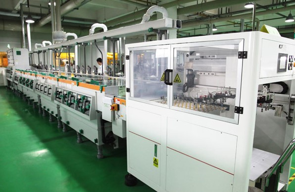
Outer dry film
11. Graphic Plating
Electroplating in PCB fabrication is pivotal for enhancing circuitry integrity and conductivity. The process uses controlled electrochemical deposition to precisely coat designated board areas with a substantial copper layer. Electroplating not only reinforces trace and pad conductivity but also enables creation of fine features per the design specifications.
At Highleap, we execute electroplating with meticulous care and precision. This enhances the overall durability and electrical performance of the finished PCB. Our expertise in electrochemical deposition produces circuit boards with robust, reliable circuitry engineered for functionality.
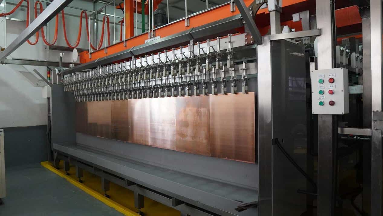
Graphic Plating-PCB Equipment
12. Etch outer layer
Outer layer etching in PCB manufacturing is critical for refining the circuitry pattern on the board surface. The controlled chemical process removes excess copper from non-designated areas, leaving precisely defined traces, pads, and interconnections. Etching creates the intended design by aligning the circuit layout precisely. It also enables intricate features and optimized track dimensions.
The meticulous orchestration of outer layer etching contributes greatly to the precision, reliability, and functionality of the final PCB product. This underscores etching’s significance in electronic systems manufacturing. Proper etching technique is essential for boards that meet design specifications.
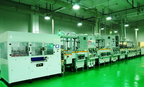
Etching equipment
13. Outer layer AOI
Outer layer Automated Optical Inspection (AOI) verifies the quality of PCB conductor patterns after etching. At Highleap, advanced AOI compares imaged layers to the original design to detect deviations. This finds errors like opens, shorts, spacing violations, and pad defects early.
Highleap leverages AOI data to promptly pinpoint and address process issues through root cause analysis. We prevent flawed boards from proceeding to further processing. This feedback loop allows continuous improvement of our fabrication techniques. Implementing rigorous outer layer inspection is essential for ensuring reliable, high-performance PCBs.
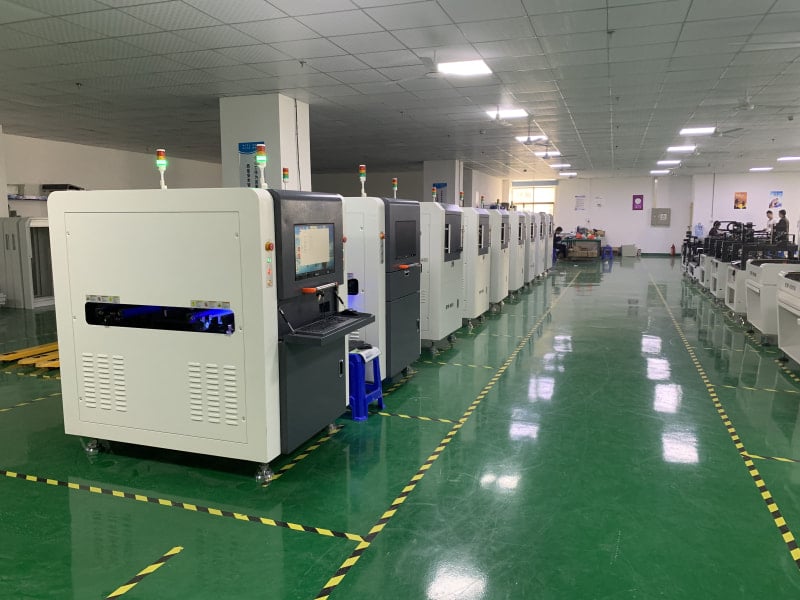
AOI
14. Soldermask
The solder mask application in PCB manufacturing plays a key role in protecting and enhancing circuitry reliability. A thin solder mask layer coats areas where soldering is not intended. This shields copper traces and components from unintended solder bridges, moisture, dust and other environmental factors. Additionally, solder mask streamlines assembly by confining solder to designated areas.
By meticulous application of solder mask, the process improves longevity, solderability, and overall quality of the final PCB. This allows seamless integration into electronic assemblies. Proper solder mask is pivotal for robust, reliable circuit boards.
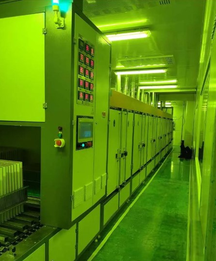
Soldermask-PCB Equipment
15. Iegend
The PCB character printing process provides clear visual identification by precisely applying labels, symbols, and alphanumeric markings. These legible and permanent markings impart crucial information like component designators, reference numbers, logos, and manufacturing details. Character printing aids assembly, debugging, and maintenance by facilitating efficient and error-free PCB handling. This enhances overall organization, traceability, and professionalism of the final product. Effective board printing and labeling enables seamless communication and operation within intricate electronic systems.
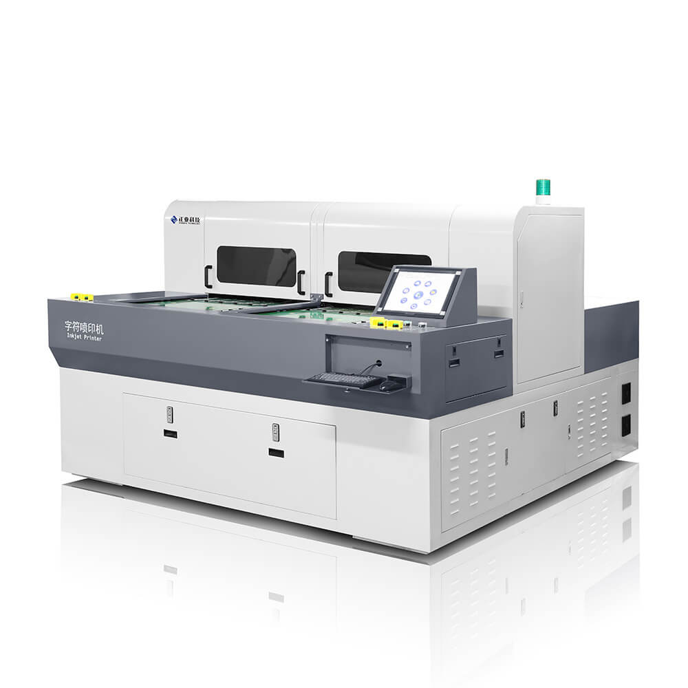
Iegend spraying machine-PCB Equipment
16. Surface Finish
Various surface finishes are applied to exposed copper regions following PCB fabrication. This serves to protect the surface and optimize solderability. Common finishes include Electroless Nickel Immersion Gold (ENIG), Hot Air Solder Leveling (HASL), and Immersion Silver. Each finish is applied in carefully controlled thicknesses and tested for solderability to ensure quality and performance. The strategic use of surface finishes safeguards the PCB and enables reliable solder connections.
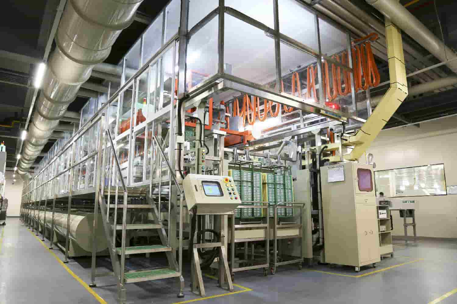
Electroless gold plate production line-PCB Equipment
17. Electronic test
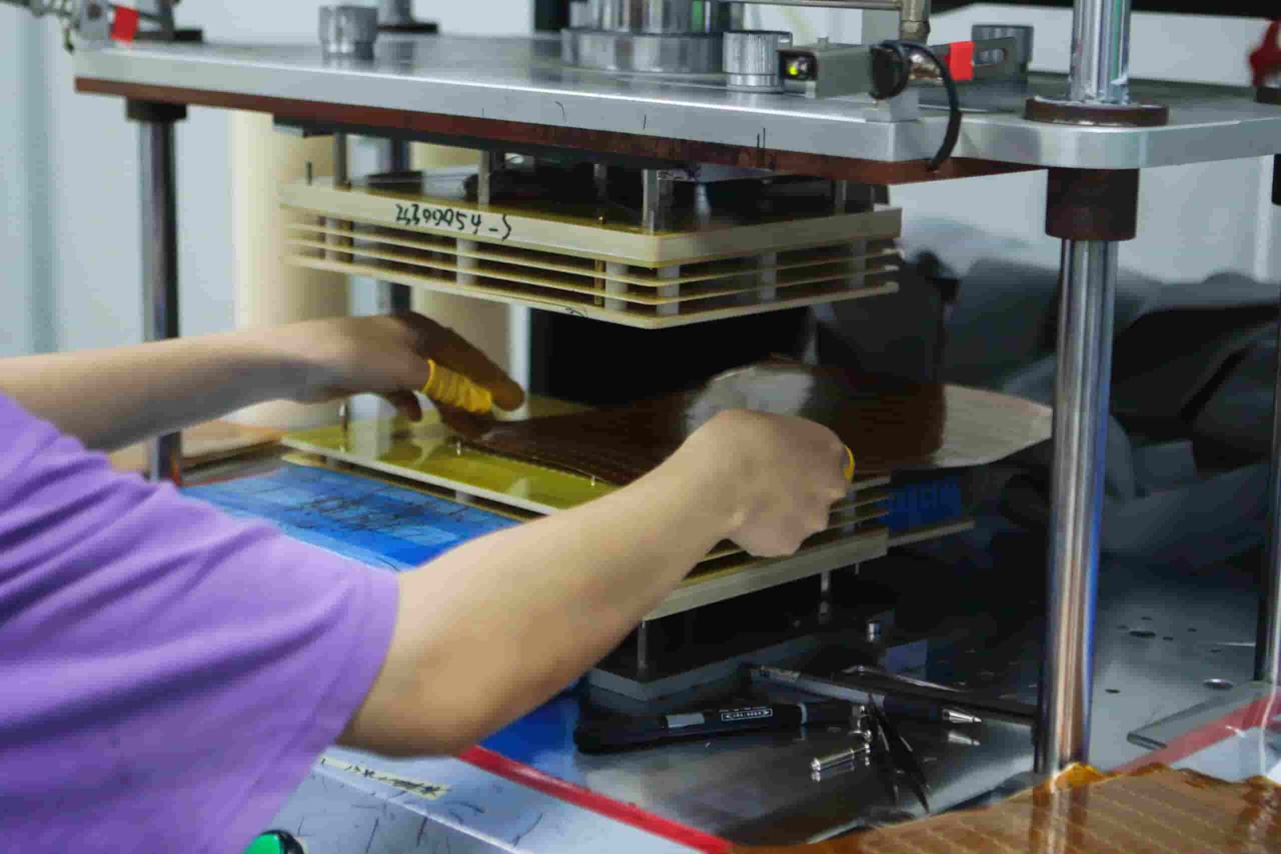
Impedance testing and electronic testing are pivotal for ensuring PCB functionality and quality. Impedance testing validates signal trace impedance, which is crucial for high-speed circuits. Precision measurements verify adherence to design specs, enhancing signal integrity.
Electronic testing assesses circuit integrity by identifying opens, shorts, and proper connectivity. Methods like flying probe and fixture testing scrutinize the board against original data to assure quality and functionality. Together, these testing phases underpin the reliability, performance, and precision of the final PCB product.
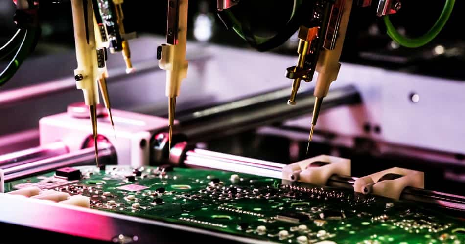
Flying probe test
Fixture test
PCB Flying Probe Test
18. Profile
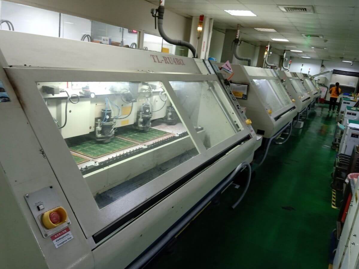
The profile stage encompasses precision cutting of manufacturing panels into designated sizes and shapes, aligning precisely with the customer’s design as outlined in the gerber data. This process offers three primary options for array provision or panel distribution: scoring, routing, or punching. Rigorously adhering to customer-supplied drawings, all dimensions undergo meticulous scrutiny to verify dimensional accuracy and compliance, ensuring that the panel attains the desired form and dimensions as per the specifications.
Milling machine
19. Final Inspection
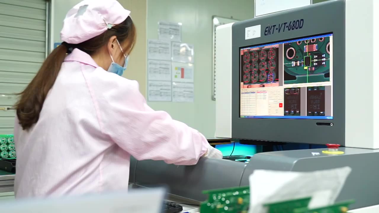
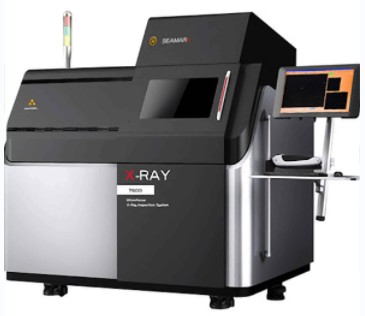
The final phase involves meticulous inspection, where each PCB undergoes rigorous visual scrutiny against acceptance criteria by qualified inspectors. Comprehensive manual and Automated Visual Inspection (AVI) is used, comparing boards to gerber data. However, human verification remains integral for accuracy.
At Highleap, every order undergoes comprehensive evaluation including dimensional analysis and solderability assessments. Our rigorous final inspection demonstrates an unwavering commitment to delivering exceptional quality PCBs that meet uncompromising standards.
First Article Inspection
PCB equipment-PCB x-ray
PCB functional test equipment
20.Reliability Test
We offer advanced PCB reliability testing equipment, including environmental test chambers, electrical testing equipment, functional testing equipment, and reliability assessment instruments. We are committed to providing customers with high-quality, highly reliable PCB solutions.
The following only shows some PCB equipment.For a complete equipment list or further information, please don’t hesitate to contact us.
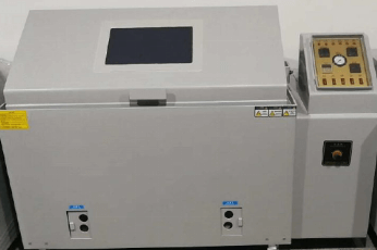
Salt spray device-PCB Equipment
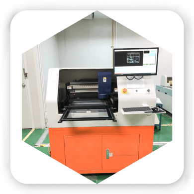
Automatic size inspection machine
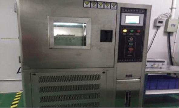
Constant temperature and humidity tester
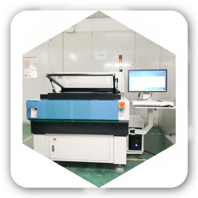
Drilling quality analysis machine
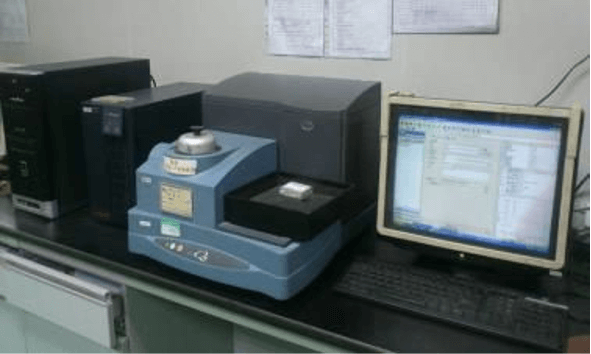
DSC for TG-PCB Equipment
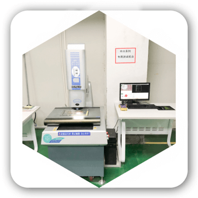
Image measuring instrument-PCB Equipment
21. Package
Packaging is the concluding phase in PCB production, encompassing meticulous procedures to safeguard the integrity of the manufactured boards. Each PCB is carefully positioned within specialized packaging materials designed to prevent physical damage, electrostatic discharge, and environmental contaminants during transit and storage. The packaging process includes considerations for factors such as board size, quantity, and specific requirements. This meticulous attention to packaging ensures that the PCBs arrive at their destination in pristine condition, ready for integration into electronic devices or systems, while upholding the quality and precision upheld throughout the entire production journey.
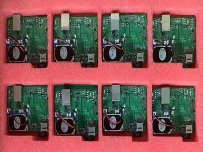
PCB-packaging-customization
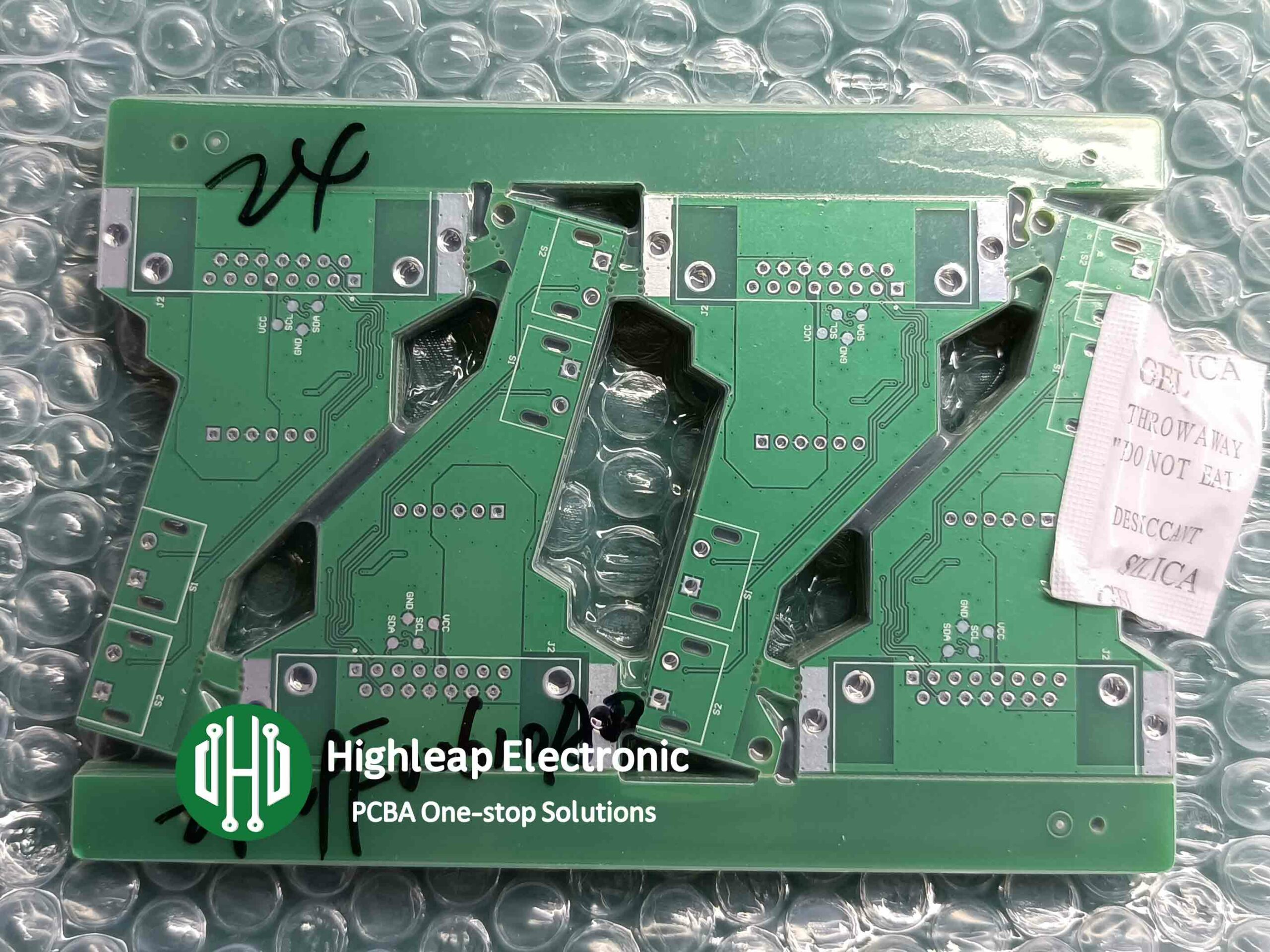
PCB-packaging
22. Finished Product Warehouse
The Finished Goods Warehouse stands as the final repository within PCB production, housing meticulously crafted and inspected circuit boards. This secure facility ensures the organized storage and protection of completed PCBs, shielding them from potential damage, environmental factors, and electrostatic discharge. Each board is methodically cataloged and stored, ready for efficient retrieval and distribution as per client requirements. The Finished Goods Warehouse embodies the culmination of the production process, safeguarding the quality and integrity of the PCBs until they are dispatched for integration into electronic systems or devices.
