PCB Assembly
Highleap Electronic offers turn-key PCB assembly services in prototype quantities or low-volume to mid-volume production runs.
From A to Z
One-stop PCBA Solution
With our expertise in both electrical and mechanical engineering, we have the capability to create comprehensive PCBA solutions that including design for assembly (DFA) check, PCB Manufacturing, component sourcing, SMT, DIP, PCBA testing, IC programming, conformal coating, electronic potting adhesive, enclosure making, finished product assembling, offering you a turnkey electro-mechanical solution tailored to your requirements.
Smallest:0.25*0.25inches
Largest:20*20inches
Water Soluble Solder Paste.
Leaded and Lead-Free
AOI Test,Electrical performance detection, X-ray Inspection, Functional Test
Technologies and equipments
Advanced PCB Assembly
Printed Circuit Board Assembly are expected to deliver enhanced functionality within increasingly compact dimensions nowadays. Achieving your desired levels of quality, performance, and speed necessitates the strategic deployment of advanced manufacturing and engineering technologies precisely when needed in the production process.
At Highleap Electronic, we have 5 SMT placement lines, 4 DIP insertion lines, 1 conformal paint spraying line, 1 glue filling line, 2 finished product assembly lines. We have separated production line for product with lead and lead-free to control the process of fabrication, testing, and shipping strictly.
BGA Capabilities
In the realm of electronics, BGA packages offer space efficiency, thermal prowess, stable electrical performance, and streamlined manufacturing, reducing costs. Highleap, a leading PCB & PCBA manufacturer, harnesses BGA’s advantages for top-quality, cost-effective solutions.
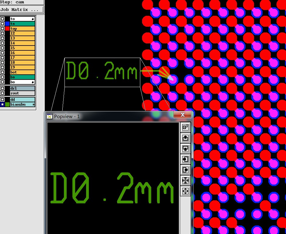
The minimum diameter of BGA pad is 0.2MM (the sample limit can be 0.15MM).
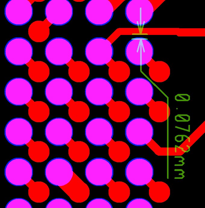
The minimum BGA to line is 3MIL (the prototype limit can be 2.5MIL).
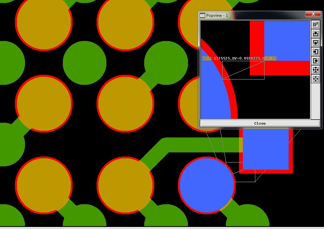
The minimum distance from the BGA solder pad edge to solder pads edge of other components is 0.15mm
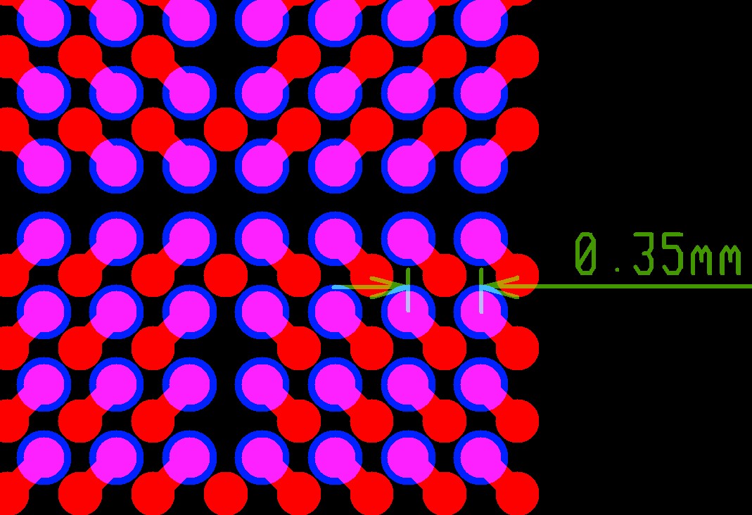
The minimum distance from the center of one BGA solder pad to the center of another BGA solder padis 0.35mm.
IC programming services
Highleap Electronic offers IC programming services that enable you to subcontract the programming of integrated circuits (IC), eliminating the complexity and substantial time commitment associated with programming.
While programming can be carried out post-SMT mounting assembly, this approach is only suitable for prototype PCB assembly. In the context of high-volume PCB assembly, pre-assembly IC programming proves to be a more competitive choice. With this option, you can take advantage of cost-effective programming, rapid turnarounds, and zero defects.
Quick Turn
High Quality PCB Assembly
Highleap Electronic provides you with one-stop PCB assembly services with excellent technology and professional team. Whether it is in prototype quantities or in small to medium-volume production runs, we can complete them accurately and efficiently. We focus on every detail to ensure that the quality and performance of PCB assembly reach the optimum. Choosing Highleap Electronic means choosing reliability and excellence. Let us build a solid foundation for your electronic devices and help your products stand out in the market.
100% original and genuine products
Electronic Components Sourcing
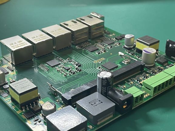
Our expertise encompasses a diverse range of sectors, including industrial control, military applications, security systems, LED lighting, medical equipment, automotive electronics, instrumentation, consumer electronics, optoelectronic integration, power management, communication networks, computer circuit components, smart homes, sensing instruments, subway high-speed rail systems, and automation solutions. Our capabilities extend to serving various needs, including spot purchases, precise bill of materials matching, cost optimization, and small-batch acquisitions.
100% electrical performance testing
PCBA Testing
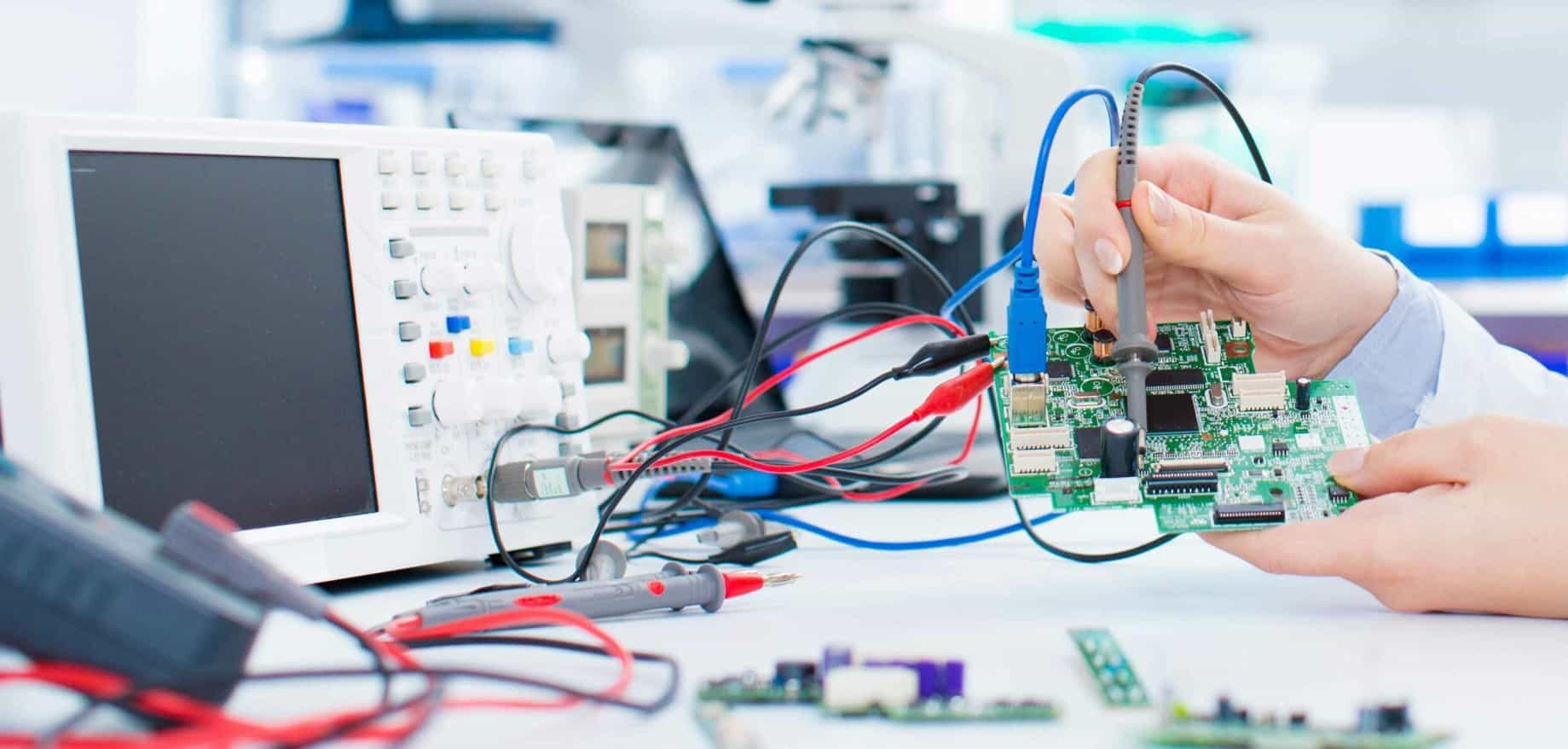
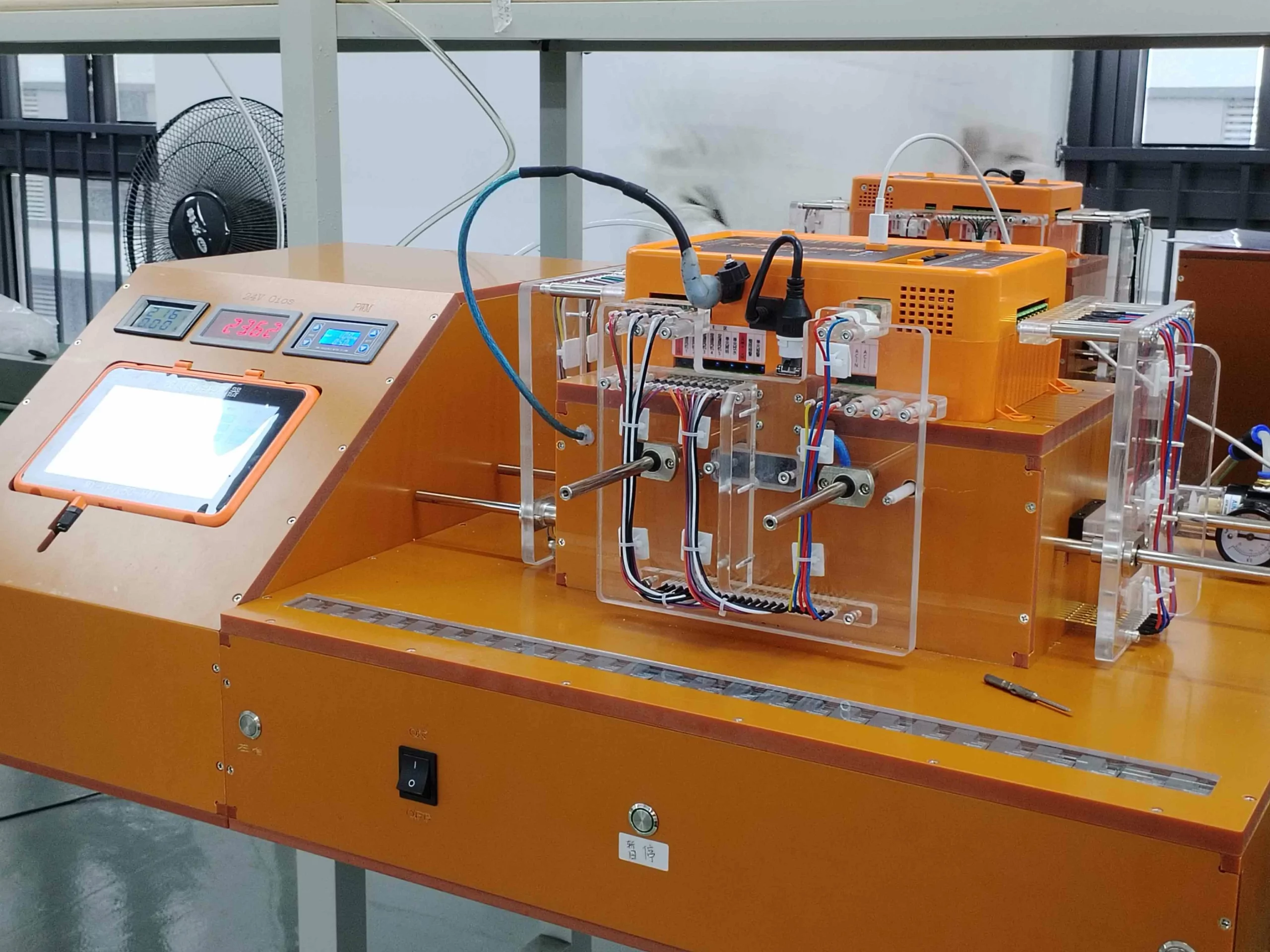
Quality assurance in the PCB assembly process is of utmost significance in guaranteeing the delivery of dependable and high-performance electronic products. At Highleap Electronic, we provide first article inspection, AOI, X-ray inspection, electrical performance testing, metallographic section analysis, and functional testing and other essential tests for your PCBA projects.
Meet a variety of needs of printed circuit boards
PCB Assembly Process Flow
1
Incoming Material Inspection
The purpose of incoming material inspection is to prevent poor quality and delay delivery from defective materials. We should make sure the PCB boards are correct and the incoming components are consistent with BOM to be soldered.
2
Solder Paste Printing
It’s a key part of PCBA process. The most widely used method for applying solder paste to a PCB is through a laser stencil printer. This process precisely deposits the right amount and thickness of solder onto the solder pads.
3
Solder Paste Inspection (SPI)
SPI enables the direct assessment of solder paste quality on PCBs and offers insights into the types of defects present. Manufacturers can leverage solder paste inspection to minimize defect rates, resulting in substantial cost and time savings.
4
SMD Component Placement
In the Surface Mount Device (SMD) phase, automated machines meticulously place components on the solder paste. This step requires high precision, as even a minor misalignment can lead to faulty connections.
5
Reflow Soldering
The assembled PCB then enters the reflow soldering oven. In this controlled environment, the solder paste melts and solidifies, forming secure connections between the components and the PCB.
6
Automated Optical Inspection (AOI)
Quality control is paramount. AOI systems use cameras to examine the solder joints and components for defects. Any inconsistencies are flagged, and corrective measures are taken.
7
Repair
PCBs that do not pass AOI inspection will be forwarded to maintenance personnel for rework. Rework is carried out using tools such as soldering irons and repair workstations to rectify the identified problems.
8
Through-Hole Component Soldering
Through holes are drilled into the PCB, and components are manually or automatically inserted. These components are then soldered from the opposite side, ensuring robust connections.
9
Wave Soldering
The PCBs are conveyed over a bath of molten solder, allowing the soldering surfaces of the through holes to directly connect with the molten solder.
10
X-Ray Inspection
X-ray inspection becomes critical if there are components such as quad flat no-leads (QFN) and ball grid arrays (BGA) on the printed circuit board. This method can uncover hidden assembly defects that may not be visible through standard visual inspection.
11
First Article Inspection
During this stage, various data such as the BOM, coordinates, designators, or sample images are inputted into the application to create a test program.
12
IC Programming
Following PCBA production, there are multiple methods available for IC programming. Highleap ELectronic provides offline programming and online programming.
13
Functional Test
Functional test assesses the PCB’s functionality, ensuring that it meets expected electrical characteristics and performs as intended.
14
Visual Inspection
Visual inspection of the assembled board must adhere to the IPC – 610 inspection standard. This standardizes the inspection process for finished products, guaranteeing soldering quality and preventing the shipment of defective boards.
15
PCBA Cleaning
In the final production of Printed Circuit Boards, a cleaning process is essential to eliminate soldering residue like flux, dust, and solder beads from the assembled PCB. Once cleaning is complete, we can proceed to the next step of packaging.
16
PCBA Packing
Before shipping, it is imperative to employ specialized packaging for PCBA to safeguard against damage during transit and guarantee the pristine condition of the final PCBA board upon delivery to the customer.
Certifications
ISO 9001
Highleap electronics has ISO9001 2015 certification, adhering to the concept of continuous improvement of products and services to meet and exceed customer expectations.
ISO 13485
We leverage our years of experience, our state-of-the-art processes and facilities, and our passion for what we do to build the best PCBAs for the medical equipment industry.
IATF16949
Highleap Electronic guarantees automotive products’ quality and security and help clients improve the performance and reliability of automotive products.
UL
With UL certificated, Highleap Electronics has been promoting testing capabilities and up to now, we’re capable of carrying out first article inspection, AOI, X-ray inspection, etc.
Office
Room 1905,Building 2, Changfeng International,
Xintang Town, Zengcheng District,
Guangzhou,China
Email:Angel@hilelectronic.com
Phone: +86 13503062089
R&D Center
Room 201, Building A, No. 1, Qianwan 1st Road, Qianhai Shenzhen-Hong Kong Cooperation Zone, Shenzhen
Email:Howard@hilelectronic.com
Phone: +86 13500039316
PCB Factory
Room 501, Tianfucheng Business Center, No. 258 Yongfu Road, Tangwei Community, Fuhai Street, Baoan District, Shenzhen
Email:Cindy@hilelectronic.com
Phone: +86 18903006645
PCBA Factory
Building C03, Ping An Technology Silicon Valley, No. 76, Chuangyu Road, Ningxi Street, Zengcheng District.
Email:Ashley@hilelectronic.com
Phone: +86 18928950984
Take a Quick Quote
Discover how our expertise can help with your PCBA project.
