PCB Design Rule Check (DRC)
Explore PCB Design Rule Check (DRC) to Elevate Your Projects. Ensure Error-Free Designs, Optimize Manufacturability, and Enhance Electrical Performance.
What is PCB Design Rule Check
PCB design and manufacturing are intricate, involving thousands of components and connections on multilayer boards. To boost production yields and maintain quality, Design Rule Check (DRC) is vital. DRC identifies and fixes errors early in the design phase, preventing product wastage caused by issues like shorted power grounds, misaligned vias, or missing pins. It’s crucial for upholding PCB quality in production.
PCB Design Rule Check (DRC) is an essential step in the PCB design flow to verify that the layout meets pre-defined design rules and manufacturing requirements. Also known as DRC in the PCB industry, it serves two key purposes:
1. Assess PCB layout against various design rule checks – DRC tools perform extensive checks related to spacing, widths, etc. of the PCB layout objects like traces, vias, pads, etc. This ensures the design adheres to fabrication and assembly requirements prescribed by the PCB manufacturer.
2. Verify manufacturing compatibility – DRC examines the Gerber data files generated from PCB design software against the manufacturing capabilities of the PCB fabrication house. This validation eliminates errors and prevents potential manufacturing issues.
PCB Design Rule Check (DRC) is an indispensable tool in modern PCB design, ensuring that the final design meets quality, performance, and manufacturability standards. It plays a critical role in preventing design errors, minimizing manufacturing issues, and ultimately contributing to the successful development of electronic products.
Combination of PCB DRC and PCB Layout
In the realm of PCB design, the fusion of PCB Design Rule Check (DRC) and the PCB layout process has ushered in a new era of efficiency and precision. This seamless integration allows for a streamlined workflow, reducing manual tasks and ensuring design compliance. Here’s how this combination works:
Integrated DRC Rules
PCB Design Rule Check (DRC) rules are meticulously categorized into specific areas like Signal Integrity (SI), Power Integrity (PI), Electromagnetic Interference (EMI), and safety. Each rule is thoughtfully accompanied by a comprehensive descriptive overview page, greatly simplifying the process of selecting and conducting crucial tests for the PCB layout. This feature ensures that designers can navigate and verify their designs with unparalleled ease and precision, contributing to a robust and efficient design validation process.
Identifying Impedance Discontinuities
High-speed nets crossing split planes can introduce impedance discontinuities on signal traces, potentially causing issues such as reflections, radiation, and crosstalk.
Manually identifying and reviewing all such instances in complex PCB designs is a daunting task.
Traditional simulation tools often overlook these occurrences.
However, the “nets crossing gaps” rule in DRC efficiently identifies and locates these discontinuities, enhancing the design process’s efficiency.
PCB DRC Running
After running a PCB Design Rule Check (DRC) rule, designers can conveniently access a dedicated spreadsheet tab displaying detailed results for that specific DRC test. By simply clicking on a violation within the spreadsheet, the tool instantly highlights the precise location of the error on the PCB design. Furthermore, any associated parts or traces linked to the violation are also thoughtfully highlighted, providing quick and comprehensive reference for efficient error resolution.
Streamlined Workflow
The integration of PCB layout and PCB Design Rule Check (DRC) interfaces ensures that violation data seamlessly loads into the PCB layout tool.
PCB designers no longer need to manually cross-reference between different tools, enhancing workflow efficiency.
When changes are made to the PCB design to address violations, the linked DRC client can be used directly within the layout tool window to rerun selected rules and ensure that violations are cleared.
What Does a Design Rule Check (DRC) Include
A comprehensive Design Rule Check (DRC) is the cornerstone of a successful PCB design, aligning it with manufacturing capabilities. At Highleap, we take pride in offering exemplary PCB and PCBA manufacturing services. Here are examples of common DRC criteria:
Minimum Track Width and Via Size
Compliance with the PCB manufacturer’s manufacturing capabilities is essential. This includes adhering to minimum track width and via size requirements.
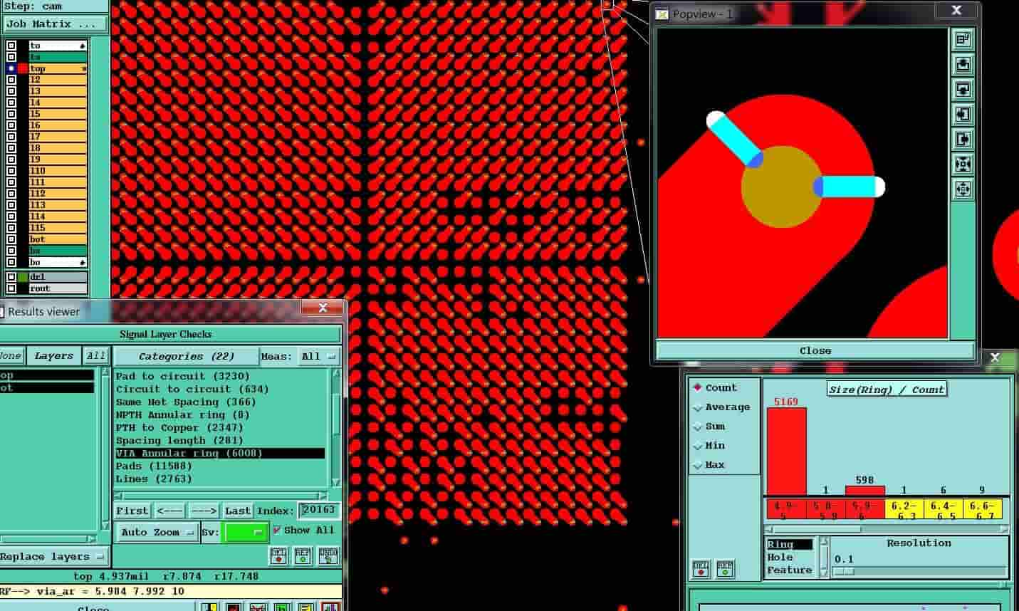
Vias annular ring checking
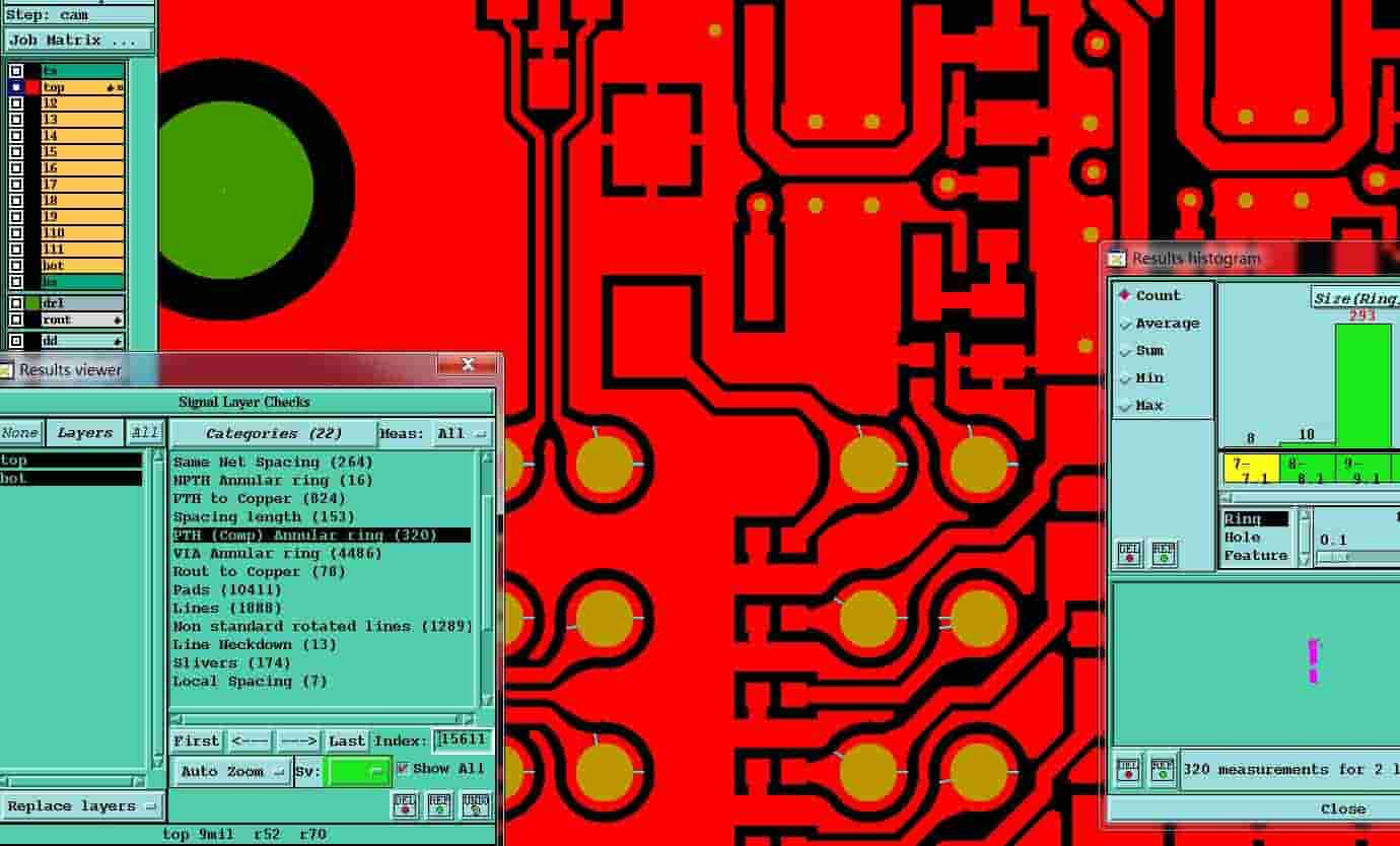
PTH annular ring checking
Spacing Considerations
Adequate spacing is crucial. This involves the spacing between tracks, tracks and pads, tracks and vias, pads and vias, and vias and vias. It is essential to meet production requirements. For instance, at Highleap, the minimum track width and spacing are 3 mil (0.0762 mm), but a recommended practice is to design with track widths and spacing of 6 mil (0.15 mm) or higher to optimize cost-effectiveness.
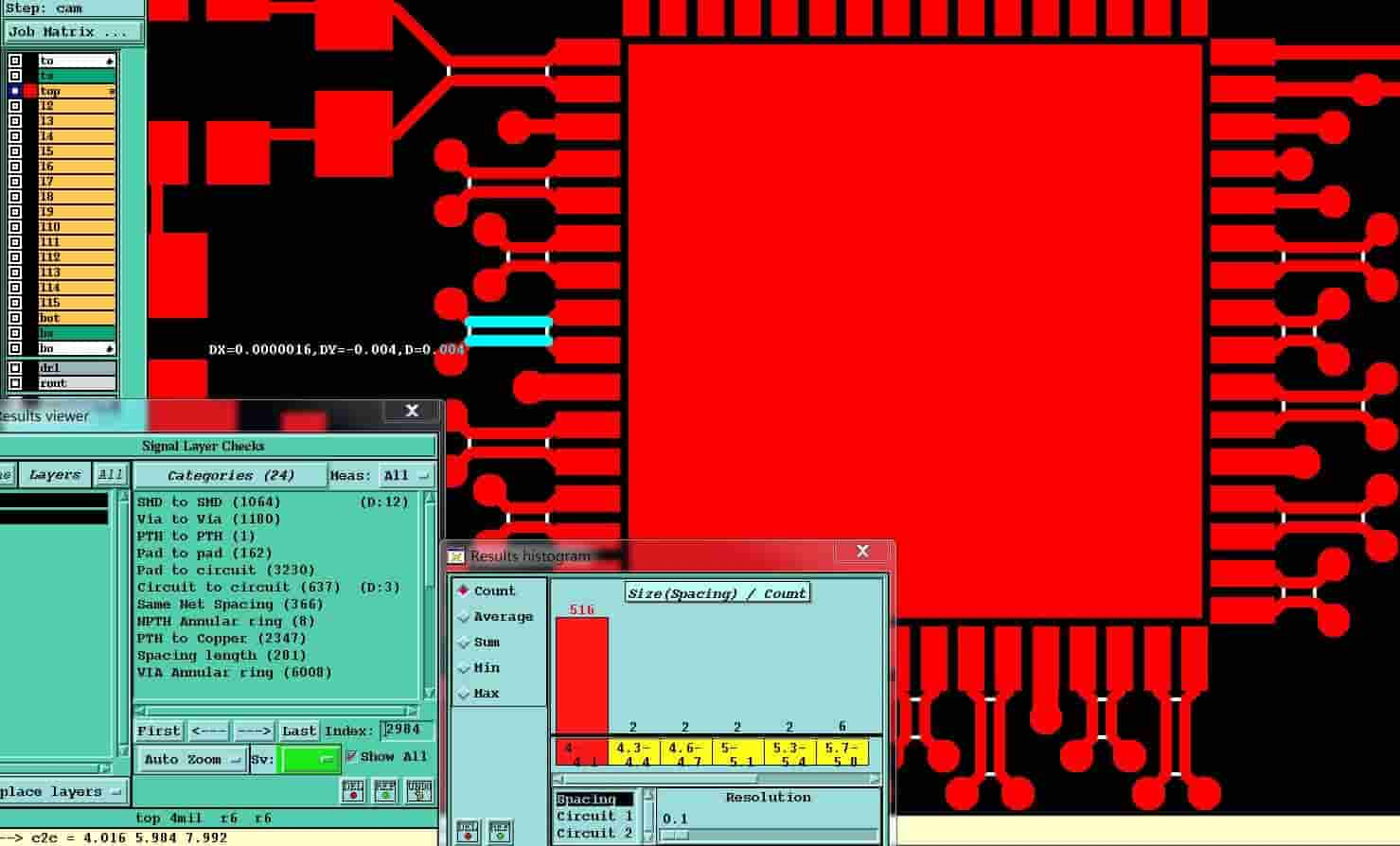
spacing checking
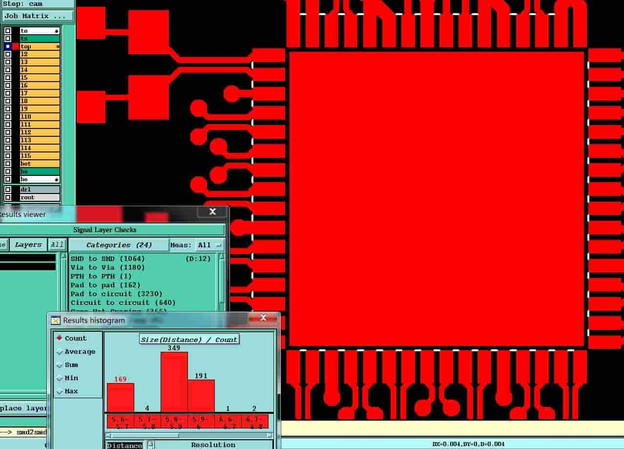
spacing checking
Power and Ground Trace Width
The width of power and ground traces should be thoughtfully determined and tightly coupled for efficient power distribution.
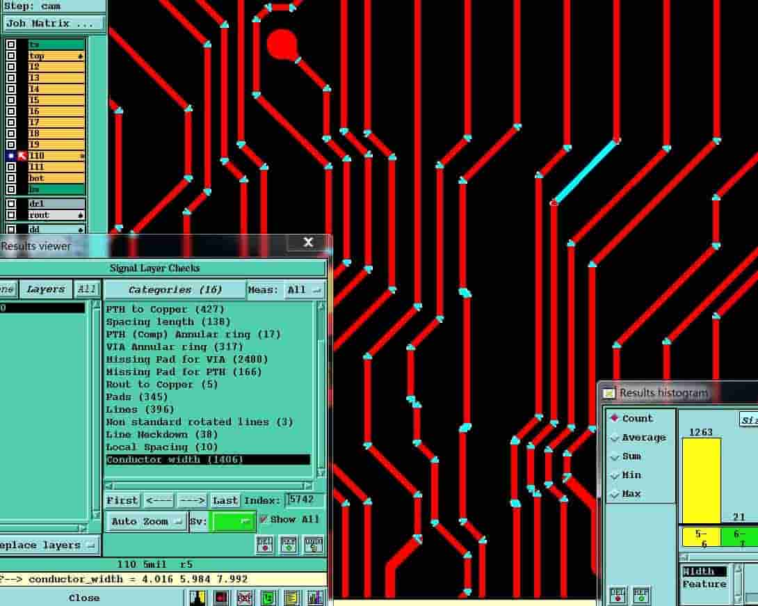
Tracks width analysis
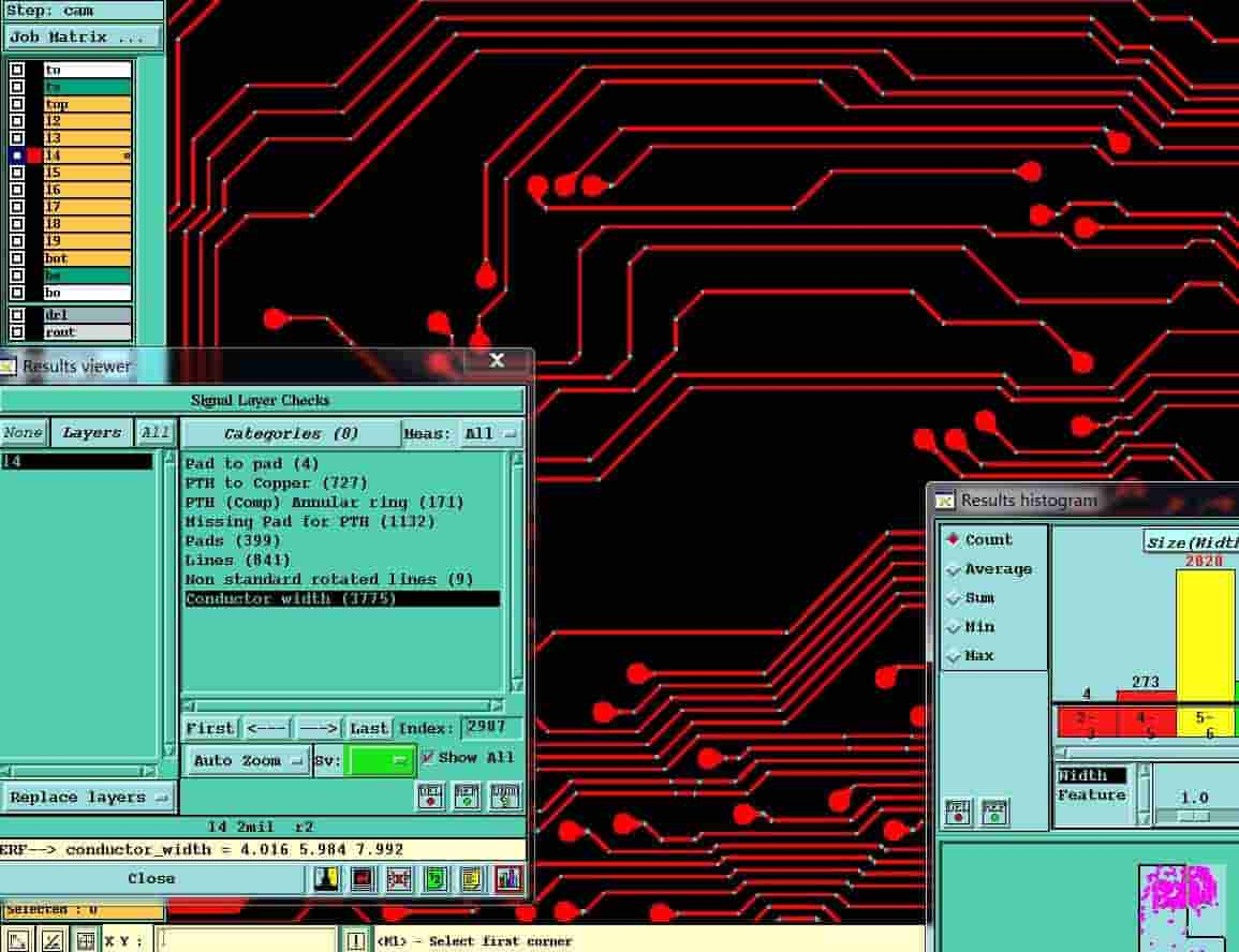
Tracks width analysis
Signal Integrity
For critical signal traces, adherence to data sheet specifications and relevant routing guidelines is crucial. This includes minimizing trace length, incorporating guard traces, and meeting impedance requirements, especially for differential pairs.
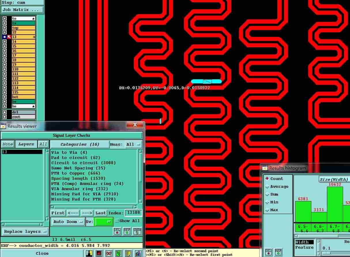
Tracks width check
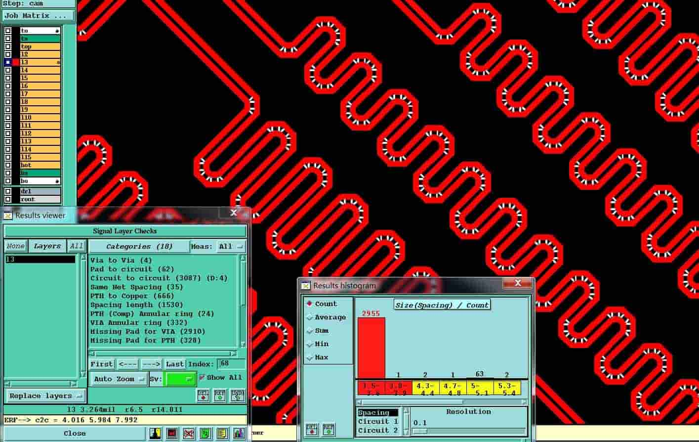
Tracks spacing checking
Signal Separation
Proper signal separation is essential. It involves separating input and output signals, digital and analog sections, high-frequency and low-frequency sections, as well as high-power and low-power sections.
These examples represent just a fraction of the checks performed during the design phase. A comprehensive DRC ensures that PCB designs meet the highest standards of quality, functionality, and manufacturability, values we uphold at Highleap as your trusted PCB and PCBA manufacturer.
Importance of PCB Design Rule Check (DRC)
Design rule checking is a critical step that verifies the manufacturability, functionality, and reliability of a printed circuit board (PCB) layout. Thorough DRC has far-reaching benefits that impact every stage of the design cycle:
- In design, DRC provides rapid feedback to engineers, enabling them to rectify issues precisely and optimize the layout. This prevents costly re-spins later.
- In fabrication, adhering to DRC guidelines results in higher yields, fewer defects, and smooth manufacturing. The PCBs fabricated are right-first-time.
- In testing, boards that pass DRC have fewer faults. Resources can be focused on functionality rather than basic faults.
- In operation, compliance with signal integrity, power integrity and EMI rules leads to reliable, robust performance in the field.
For quality assurance, comprehensive DRC signifies due diligence in design practices and reduces compliance risks. - In essence, DRC is more than just rule checking – it is vital for ensuring functional, manufacturable, high-quality PCBs that meet requirements.
Integrating DRC deeply within the design flow is key to enabling informed layout decisions and a prevention-first design mentality. The upfront investment in rigorous DRC pays dividends across the entire product lifecycle.
PCB DRC Rules
PCB Design Rule Check (DRC) encompasses a set of rules and guidelines that ensure the accuracy, manufacturability, and performance of printed circuit board (PCB) designs. These rules cover various aspects of the PCB design process and can vary depending on the specific requirements of the project and the capabilities of the PCB manufacturer. Here are some common categories of PCB DRC rules:
Dimensional Rules
- Board outline: Ensure that the PCB outline adheres to specified dimensions.
- Component placement: Define minimum and maximum component spacing, keep-out areas, and keep-in areas.
Electrical Rules
- Trace width and spacing: Specify minimum and maximum trace widths and the spacing between traces.
- Via types and sizes: Define acceptable via types and sizes, including hole diameter and annular ring dimensions.
- Impedance control: Set rules for maintaining consistent impedance for signal traces, especially for high-speed designs.
- Clearance and isolation: Specify minimum clearances between different electrical elements, such as traces, pads, and vias.
Signal Integrity (SI) Rules
- Length matching: Ensure that traces within high-speed signal paths are matched in length to minimize signal skew.
- Differential pair routing: Define requirements for routing differential pairs with controlled spacing and length matching.
- High-speed signal termination: Specify proper termination techniques for high-speed signals.
Power Integrity (PI) Rules
- Power plane continuity: Ensure a continuous power plane with appropriate via stitching for stable power distribution.
- Decoupling capacitors: Specify placement and values of decoupling capacitors to minimize power noise.
Manufacturability Rules
- Drill hole sizes and aspect ratios: Set guidelines for minimum and maximum drill hole sizes and aspect ratios to ensure manufacturability.
- Solder mask clearances: Define minimum clearances for solder mask openings to prevent solder bridging during assembly.
- Copper-to-edge spacing: Specify minimum distances between copper features and the PCB edge.
Silkscreen and Documentation Rules
- Reference designators and component outlines: Ensure that silkscreen markings are clear and correctly aligned with components.
- Assembly notes and documentation: Provide guidelines for including essential assembly and fabrication information in the PCB design.
Specialized Rules
- These rules can be project-specific and may include unique requirements based on the application or industry standards.
These rules can be project-specific and may include unique requirements based on the application or industry standards.
It’s essential to tailor DRC rules to the specific project and manufacturing process to ensure a successful PCB design. Adhering to these rules helps prevent errors, optimize manufacturability, and ensure the desired electrical performance of the final PCB.
For all your PCB and PCBA manufacturing needs, Highleap is your trusted partner. We combine cutting-edge technology with a commitment to quality, ensuring your designs become reality with precision and reliability.
