
SY S1000H PCB Fabrication & Assembly
SY S1000H is a third-party laminate material reference used in customer documentation. Highleap Electronics is a PCB fabrication and PCB assembly factory. We do not manufacture base laminate materials.
We review the approved design, the nominated construction, and production constraints so that the finished board can be built and assembled to the project requirements.
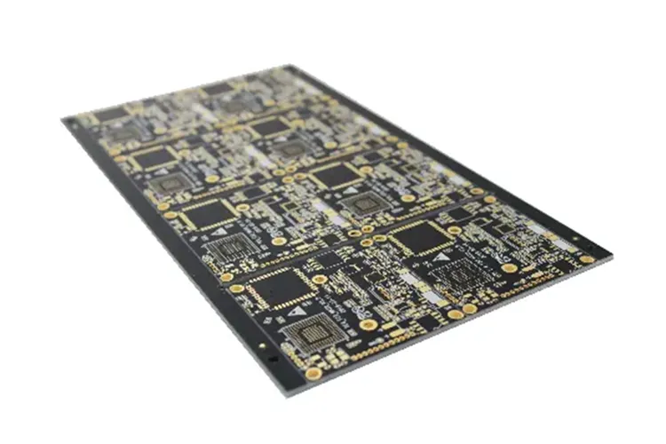
Customer-specified laminate manufacturing
What Does S1000H Mean in a PCB Specification?
When S1000H appears in an approved PCB stack-up or fabrication document, it identifies the laminate required for that board construction. Highleap Electronics manufactures the finished PCB or PCBA to the customer-approved production specification.
Our engineering review considers the complete design: Gerber or ODB++ data, layer count, dielectric construction, copper thickness, trace geometry, via structures, finished board thickness, surface finish, controlled impedance, dimensions, tolerances, and test requirements.
Material properties that affect circuit design or product qualification should be based on the customer’s approved engineering documentation and current technical data from the material manufacturer. Highleap does not manufacture the S1000H laminate.
Fabrication and assembly capabilities
How Highleap Manufactures PCBs with Customer-Specified S1000H
We review the approved board construction before production and manufacture to the agreed material, stack-up, dimensional, impedance, and fabrication requirements.
Multilayer PCB Manufacturing
Prototype and production fabrication for customer-designed multilayer PCB constructions.
Controlled Impedance
Manufacturing to customer-defined impedance targets, tolerances, and approved stack-ups.
Blind & Buried Vias
Advanced via structures reviewed against the board design and manufacturing requirements.
Via-in-Pad Structures
Suitable via-in-pad solutions for demanding component layouts and PCB designs.
Custom PCB Stack-Ups
Layer construction, dielectric thicknesses, copper requirements, and board thickness reviewed before production.
Electrical Testing
Finished bare PCBs electrically tested in line with agreed project and production requirements.
Highleap can continue from bare PCB fabrication to complete PCBA production, including component sourcing, SMT and through-hole assembly, BGA and fine-pitch assembly, AOI, X-ray inspection where required, programming, and customer-specified functional testing.
From PCB Fabrication to Complete Assembly
One manufacturing partner for PCB production, component sourcing, and PCBA assembly.
Typical applications
Applications for PCBs Specifying S1000H
Final material suitability and board construction depend on the customer’s approved design, operating environment, and product qualification requirements.
Industrial Electronics
PCB and PCBA manufacturing for control systems, automation equipment, instrumentation, and industrial assemblies.
Communication Equipment
Circuit board manufacturing for communication modules, network equipment, control boards, and related systems.
Power & Control Systems
PCB fabrication and assembly for power management, monitoring, and control electronics.
Computing & Embedded Systems
Multilayer PCB and PCBA production for embedded hardware, controllers, and data-processing electronics.
S1000H is referenced solely as a customer-specified laminate designation. Highleap Electronics is an independent PCB manufacturing and PCB assembly company; this reference does not imply manufacture of the laminate or any affiliation with its manufacturer.
Manufacturing with customer-nominated SY S1000H material
Highleap supports multilayer PCB fabrication and assembly projects with nominated material requirements. The useful starting point is a complete fabrication package, rather than a generic material claim: stackup drawing, layer data, drill chart, impedance requirements, and the intended assembly process.
For this type of program, our engineering attention is directed to stackup coordination, hole reliability, and production-ready documentation. The final construction is reviewed against the actual board design, availability, and the customer-approved document set.
Project review inputs
Before fabrication release, our CAM team reviews material callout, construction drawing, copper weights, drill chart, assembly conditions, and inspection needs. Clear input at this stage helps avoid last-minute construction changes and gives purchasing, fabrication, and assembly teams the same project baseline.
Where a material callout is critical, please identify the exact construction and approved source documentation in the order package. We can then confirm manufacturability and propose practical board-level alternatives if the nominated construction is unavailable.
Engineering planning checklist
| Review area | Project input | Manufacturing focus |
|---|---|---|
| Construction | Approved stackup and finished thickness | Layer registration and build planning |
| Copper and routing | Weights, controlled nets, and plane requirements | Etch compensation and signal reference continuity |
| Holes and features | Drill chart, via type, and tolerances | Drill, plating, and inspection sequence |
| Assembly | Component, finish, and process constraints | Profile planning and fit verification |
| Acceptance | Test and documentation requirements | Inspection records for the agreed build |
This checklist is fabrication guidance, not a substitute for the material owner’s current technical documentation.