
F4B Teflon PCB Laminates – Microwave PCB Manufacturer | Highleap Electronics
Highleap Electronics provides F4B PTFE PCB manufacturing and assembly for RF, microwave, antenna, radar, and communication designs using specified Wangling high-frequency laminate grades.
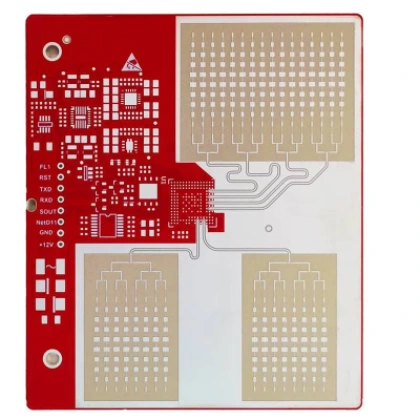
F4B PTFE PCB Manufacturing for RF and Microwave Designs
F4B refers to a family of PTFE-based, glass-fabric-reinforced microwave laminate materials used in RF and high-frequency circuit boards. Taizhou Wangling Insulating Materials Factory lists F4B within its PTFE woven-fiberglass substrate portfolio and also offers newer related material families for different dielectric, copper-foil, and RF requirements.
Highleap Electronics provides PCB fabrication and PCB assembly services for projects using F4B and other PTFE-based high-frequency materials. Typical manufacturing requirements include controlled transmission-line geometry, dielectric thickness, copper construction, plated-hole preparation, dimensional control, surface finish, and RF assembly interfaces.
F4B-based PCBs may be considered for antenna circuits, radar electronics, RF passive networks, microwave communication hardware, phase-control circuits, and other applications where dielectric properties and transmission-line behavior are important to the electrical design.
- PTFE-based RF and microwave PCB fabrication
- Controlled-impedance transmission-line structures
- Antenna, radar, and RF passive circuit boards
- Single-sided, double-sided, and selected multilayer constructions
- RF PCB assembly and component integration
- Support for approved Wangling high-frequency material grades
Wangling F4B, F4BM and F4BME Material Families
Wangling’s high-frequency material portfolio includes the original F4B series together with later PTFE woven-glass laminate families such as F4BM and F4BME. These designations should be treated as separate material grades rather than interchangeable names, because their dielectric ranges and copper constructions differ.
According to Wangling’s current product information, F4BM and F4BME use the same general dielectric family but different copper-foil constructions. F4BM is paired with ED copper foil, while F4BME uses reverse-treated RTF copper foil for designs where conductor characteristics and PIM-related requirements are relevant.
The current F4BM/F4BME portfolio covers multiple dielectric-constant grades from approximately 2.17 to 3.00. The exact material model, Dk, Df, copper type, laminate thickness, and construction should therefore be specified before PCB fabrication rather than referring only to “F4B.”
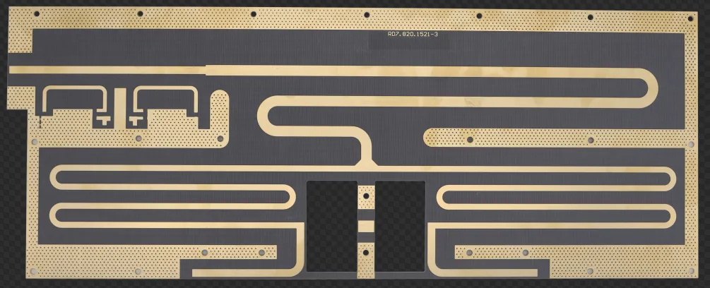
Detailed Technical Specifications of F4B-1/2 Teflon PCB
| Property | Test Condition | Unit | Value |
|---|---|---|---|
| General Information | |||
| Appearance | Meet the specification requirements for the laminate of microwave PCB by National and Military Standards. | ||
| Types | F4B255 / F4B265 | ||
| Dielectric Constant | 2.55 / 2.65 | ||
| Dimension (mm) | 300×250, 380×350, 440×550, 500×500, 460×610, 600×500, 840×840, 1200×1000, 1500×1000 | ||
| Note | For special dimension, customized laminates are available. | ||
| Copper Thickness | 0.035 μm / 0.018 μm | ||
| Thickness and Tolerance | |||
| Laminate Thickness (mm) | 0.17, 0.25 | 0.5, 0.8, 1.0 | 1.5, 2.0 | 3.0, 4.0, 5.0 | ||
| ±0.025 | ±0.05 | ±0.05 | ±0.09 | |||
| Note | Includes copper thickness. Customized options available. | ||
| Mechanical Strength | |||
| Maximum Warp (mm) | Thickness 0.25–0.5: 0.030 (original), 0.050 (single), 0.025 (double) Thickness 0.8–1.0: 0.025 / 0.030 / 0.020 Thickness 1.5–2.0: 0.020 / 0.025 / 0.015 Thickness 3.0–5.0: 0.015 / 0.020 / 0.010 |
||
| Cutting Strength | 1 mm board, no burrs after cutting, min. hole spacing 0.55 mm, no delamination. | ||
| Punching Strength | 1 mm board, no burrs after punching, min. hole spacing 1.10 mm, no delamination. | ||
| Peel Strength (1oz copper) | ≥15 N/cm (normal), ≥12 N/cm (constant humidity & temp), solder 260°C ±2°C for 20s | ||
| Chemical Property | |||
| Chemical Resistance | Etching applicable, dielectric properties unchanged. For plated-through holes, sodium or plasma treatment required. | ||
| Electrical Property | |||
| Density | Normal state | g/cm³ | 2.2 ~ 2.3 |
| Moisture Absorption | 24 h in distilled water @ 20±2°C | % | <0.1 |
| Operating Temperature | High-low temp chamber | °C | -50 ~ +260 |
| Thermal Conductivity | – | W/m·K | 0.3 |
| CTE (typical) | 0~100°C | ppm/°C | 16(x), 21(y), 186(z) |
| Shrinkage Factor | 2 h in boiling water | % | 0.0002 |
| Surface Resistivity | 500V DC | MΩ | ≥1×10⁴ (normal), ≥5×10³ (humid) |
| Volume Resistivity | – | MΩ·cm | ≥1×10⁶ (normal), ≥9×10⁴ (humid) |
| Pin Resistance | 500V DC | MΩ | ≥5×10⁴ (normal), ≥5×10² (humid) |
| Surface Dielectric Strength | 1 mm thick | kV/mm | ≥1.2 (normal), ≥1.1 (humid) |
| Dielectric Constant | 10 GHz | εr | 2.55, 2.65 (±2%) |
| Dissipation Factor | 10 GHz | tgδ | ≤1×10⁻³ |
Notes:
In addition to our F4B-1/2 series, Highleap Electronics specializes in a wide range of advanced PCB technologies, including:
- RF & Microwave Hybrid PCBs
- High Frequency PTFE & Teflon Circuit Boards
- FR4 Double-Sided and Multilayer PCBs
- 1–3+N+3 HDI / Any-Layer HDI PCBs
- Rigid-Flex PCBs with blind and buried vias
- PCBs with blind slots and backdrilling
- Heavy Copper PCBs for high current applications
Have questions or need a quote? Don’t hesitate to reach out to us at www.hilelectronic.com – our team will respond as soon as possible.
Related Wangling High-Frequency PCB Material Families
Wangling offers several high-frequency substrate families in addition to the original F4B material. These families use different reinforcement systems, fillers, copper constructions, and dielectric ranges, so they should be evaluated as separate material options rather than as equivalent F4B grades.
- F4BM / F4BME: PTFE woven-glass laminates available in multiple dielectric-constant grades.
- F4BTM / F4BTME: Ceramic-filled PTFE woven-glass material families.
- F4BTMS: PTFE-based ceramic-filled laminates using ultra-thin, fine woven-glass reinforcement.
- F4BXW: PTFE material family reinforced with short glass fibers.
- TFA: PTFE ceramic-filled substrate family.
- WL-PP: Bonding materials intended for selected multilayer high-frequency PCB constructions.
The appropriate grade depends on the required dielectric properties, copper construction, PCB stack-up, operating frequency, dimensional requirements, and fabrication process.

Why the Exact F4B Material Grade Matters Before PCB Fabrication
“F4B PCB” is often used as a broad description for PTFE-based microwave circuit boards, but the material designation alone does not fully define the PCB construction. Different F4B-related grades can have different dielectric constants, loss values, copper types, thickness options, and dimensional behavior.
Before production, the fabrication package should identify the exact laminate model whenever possible. This is particularly important for RF filters, antenna feed networks, couplers, power dividers, phase shifters, and other circuits in which transmission-line dimensions are calculated around a specific dielectric structure.
- Exact material model and dielectric constant
- Laminate or dielectric thickness
- Copper-foil type and finished copper thickness
- Controlled-impedance or RF line requirements
- Board dimensions and mechanical tolerances
- Via, grounding, and plated-hole structures
- Surface finish and solder-mask requirements
- Assembly documentation for PCBA production
Highleap Electronics provides F4B-series PTFE PCB manufacturing and PCB assembly based on the approved material callout and released fabrication documentation. For designs referencing an older or incomplete F4B designation, the exact material construction should be clarified before production.
Submit your F4B PCB files for manufacturing review and quotation
Related Post
Explore more related materials information.
Get a Quick Quote
Partner with Highleap Electronic for your project!
PCB Engineering Support
Support for stack-up, impedance, and RF PCB design.