
S1150G Halogen-Free PCB Manufacturing and Assembly Services | Highleap Electronics
Highleap Electronics provides S1150G halogen-free PCB manufacturing and SMT assembly. RoHS, REACH, UL 94V-0 compliant. Fast, reliable, and export-ready.
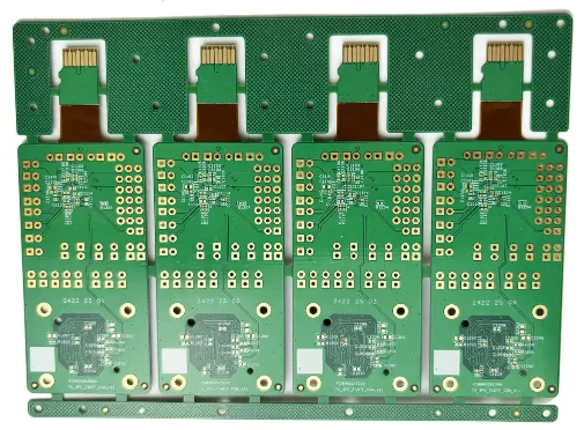
PCB Manufacturing & Assembly for Designs Specifying S1150G
Highleap Electronics provides PCB fabrication and PCB assembly services for customer projects that specify S1150G halogen-free laminate. We manufacture the finished PCB according to customer-approved Gerber files, stack-up, material callout, fabrication notes, and assembly requirements.
S1150G is a halogen-free, mid-Tg PCB laminate from Shengyi Technology. On this page, the material designation is referenced for PCB engineering and customer-specified material identification. Highleap Electronics does not manufacture S1150G or other PCB laminate materials.
Halogen-Free PCB Fabrication & SMT Assembly
For projects specifying S1150G, our engineering and production teams review the material requirement together with the complete PCB construction before fabrication. The manufacturing process is then planned around the approved board design, layer structure, drilling requirements, surface finish, and assembly documentation.
- Multilayer PCB fabrication with customer-specified S1150G material requirements
- Blind/buried vias, controlled-impedance structures, and complex PCB stack-ups
- Surface finishes including OSP, ENIG, lead-free HASL, and other specified finishes
- SMT assembly for BGA, QFN, LGA, and other component packages
- PCB inspection, electrical testing, and optional PCBA functional testing
Material availability and final PCB construction are confirmed according to each project before production. For current S1150G material properties, certifications, and compliance information, please refer to the material manufacturer’s latest official documentation.
PCB Applications Where S1150G May Be Specified
S1150G may be specified in PCB projects for consumer electronics, communication equipment, automotive electronics, display and LED products, and other multilayer electronic assemblies where a halogen-free laminate is required by the design or procurement specification.
The laminate designation alone does not determine the performance of the finished PCB. Board thickness, copper distribution, layer structure, plated-hole design, component density, operating conditions, and assembly process should also be considered when defining the final PCB construction.
- Multilayer PCBs for communication and networking equipment
- Automotive electronic control and interface boards
- Consumer and smart electronic products
- LED, display, and compact electronic assemblies
- Halogen-free PCB projects with customer-defined material requirements
Engineering Considerations for S1150G PCB Projects
When S1150G is specified in a PCB drawing or stack-up, Highleap reviews the complete board design from a manufacturability perspective. The engineering focus is on how the specified laminate works within the actual PCB structure rather than on changing or representing the material itself.
Important project inputs include layer count, core and prepreg arrangement, copper construction, finished board thickness, hole structure, controlled-impedance requirements, and the thermal demands of the intended assembly process. These details are reviewed before fabrication so that the approved material callout remains consistent with the production build.
- Multilayer PCB stack-up and thickness review
- Copper weight and layer construction planning
- Through-hole, blind-via, and buried-via requirements
- Controlled-impedance and signal-reference structures
- Surface finish, solder mask, and assembly interface review

S1150G PCB Manufacturing & Assembly with Highleap Electronics
For customer designs specifying S1150G, Highleap Electronics provides PCB fabrication and PCB assembly services based on the approved Gerber files, stack-up, material callout, fabrication notes, BOM, and assembly documentation.
Our production scope can cover multilayer PCB fabrication, drilling, plating, imaging, solder mask, surface finishing, profiling, inspection, and electrical testing. For assembled products, PCB fabrication can be coordinated with component sourcing, SMT assembly, THT assembly, inspection, and functional testing requirements.
- Prototype and volume multilayer PCB fabrication
- HDI and controlled-impedance PCB requirements
- ENIG, OSP, lead-free HASL, and other specified surface finishes
- SMT and THT PCB assembly
- Inspection, electrical testing, and production documentation
Material availability and final PCB construction are confirmed according to each project before production. Third-party material names such as S1150G are referenced only to identify customer-specified PCB material requirements.