
How to Prepare Your PCB Design for Manufacturing
Double Check Footprints and Packages
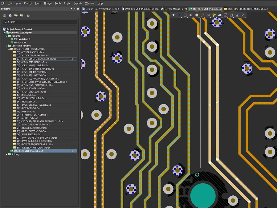
When preparing a PCB design, ensuring the accuracy of footprints and packages is crucial. Here’s a streamlined guide to optimize the process:
1. Dimensional Consistency:
- Ensure the footprint’s dimensions align with the design units, be it millimeters or mils.
- Check that the footprint dimensions specified in your design (mm or mil) match the units used in the component’s datasheet. Ensure consistency between the footprint and the datasheet to avoid any dimension-related discrepancies.

2. Datasheet Comparison:
- Cross-reference the component’s datasheet with your design footprint.
- Examine orientation, pin layouts, pad sizes, and other physical details.
- Heed any datasheet-specific notes or footprint recommendations.
3. Utilize Design Tools:
- Use projection and dimension lines in your design software for a visual match between the footprint and mechanical drawings.
- Align the footprint’s outline with the component package’s specifications.
4. Schematic and Footprint Mapping:
- Ensure the schematic symbol and footprint correspond accurately.
- Be vigilant for common errors like swapped pins or misaligned pin assignments. Ensure pin numbers and functions are consistent between the schematic and footprint.
5. Polarity Markings:
- Ensure clarity in polarity markings, including pin 1 indicators, diode cathodes, and capacitor polarity signs.
- These markings should be consistent in both the schematic symbol and footprint.
By meticulously following these steps, designers can mitigate potential footprint-related errors, ensuring accurate component placement and functionality. This diligence reduces the likelihood of manufacturing or operational challenges.
Select Pre-Tested Part Substitutions
Selecting pre-tested part substitutions and building prototypes with substitute parts can be a valuable strategy in mitigating risks associated with part shortages or unavailability. Here’s how you can implement this approach effectively:
1.Identify Critical Components and Potential Substitutes
- Identify the critical components in your design that are on critical paths and may be prone to part shortages or availability issues.
- Research and compile a list of potential substitute components that can serve as replacements for the critical components.
- Look for substitutes with similar electrical characteristics, pin configurations, and package sizes to ensure compatibility.
2.Pre-Test Substitute Components
- Obtain samples of the substitute components and conduct rigorous testing to evaluate their performance and compatibility with your design.
- Test the substitute components under various operating conditions to ensure they meet the required specifications and perform reliably.
- Assess factors such as electrical performance, thermal characteristics, and compatibility with other components in the circuit.
3.Build and Test Prototypes
- Incorporate the substitute components into prototypes of your PCB design, focusing on the critical paths where the original components would have been used.
- Test the prototypes thoroughly to verify the functionality and performance of the substitute components.
- Compare the performance of the substitute components with the original components, paying attention to any differences or limitations observed.
By following these three steps, you can establish a system of pre-tested part substitutions, allowing you to quickly adapt your design in case of part shortages. This approach helps mitigate risks and ensures the continuity of your manufacturing and production processes.
Carefully Layout Wireless Antennas
Carefully laying out wireless antennas is crucial for optimal performance and signal integrity in wireless communication systems. Here are three key points to consider:
1.Follow Recommended Layouts from the Wireless IC’s Datasheet
- Review the wireless IC’s datasheet for specific guidelines and recommendations regarding antenna layout.
- Pay attention to the suggested antenna placement, orientation, and clearance requirements specified by the IC manufacturer.
- Follow any recommended ground plane dimensions, keep-out zones, or other layout considerations provided in the datasheet.
2.Match Impedance between Transceiver and Antenna
- Ensure that the impedance of the antenna matches the impedance specified by the wireless transceiver.
- Use impedance matching techniques, such as matching networks or transmission line techniques, to achieve impedance matching.
- This ensures maximum power transfer between the transceiver and the antenna, optimizing signal transmission and reception.
3.Perform Pre-Compliance Testing
- Conduct pre-compliance testing to catch potential issues early in the design process.
- Use specialized test equipment or software tools to evaluate the antenna’s performance, including parameters such as return loss, radiation pattern, and efficiency.
- Pre-compliance testing helps identify any deviations from desired characteristics, allowing you to make necessary adjustments before finalizing the design.
By carefully following these guidelines, you can ensure an effective layout for wireless antennas, optimize signal performance, and minimize the risk of issues during the development and testing stages. This attention to detail contributes to the overall success of wireless communication systems.
Include Adequate Decoupling Capacitors
ncluding adequate decoupling capacitors is crucial for maintaining stable power supply and minimizing noise in electronic circuits. Here are two important points to consider when incorporating decoupling capacitors:
1.Place Capacitors Close to Power Pins
- Position decoupling capacitors as close to the power pins of the integrated circuit (IC) as possible.
- The proximity ensures that the capacitors can effectively filter out high-frequency noise and provide a stable power supply to the IC.
- Keep the length of the traces between the capacitors and power pins as short as possible to minimize inductance and resistance.
2.Capacitors in-line between Power Source and IC
- Connect the decoupling capacitors in-line between the power source and the IC’s power pins.
- This configuration allows the capacitors to act as a buffer, absorbing and supplying instantaneous current demands to the IC.
- Ensure that the capacitors’ positive terminals are connected to the power source, and the negative terminals are connected to the IC’s power pins.
By following these guidelines, you can effectively decouple the power supply for the IC, reducing noise and maintaining stable power delivery. Adequate decoupling capacitors help prevent voltage fluctuations and contribute to the overall performance and reliability of the circuit.
Proper Trace Widths and Spacing in PCB Design
1. Trace Width for High-Current Paths
- Ensure traces carrying high currents are adequately sized to prevent overheating.
- Utilize online trace width calculators to determine the optimal width based on the current, copper thickness, and allowable temperature rise.
2. Spacing for High-Voltage Traces
- High-voltage traces require increased spacing to prevent electrical arcing between adjacent traces.
- The spacing should be determined based on the voltage levels, safety standards, and any specific requirements of the application.
By adhering to these guidelines, you can ensure the safety and reliability of your PCB design, minimizing potential issues related to overheating or electrical shorts.
Choose the Right Power Supply Regulator Routing
Embedded systems commonly employ two major types of voltage regulators: linear regulators and switching regulators. These two types have distinct requirements and guidelines for PCB layout and routing.
Working with Linear Regulators
- Capacitor Selection: Follow the manufacturer’s guidelines for selecting the appropriate type, value, and placement of capacitors used to bypass the regulator. Typically, these capacitors should be placed as close as possible to the input and output pins of the regulator to minimize parasitic effects and ensure proper filtering.
- Heat Dissipation: Linear regulators generate waste heat, so it’s crucial to select a regulator package that can handle the expected heat dissipation. Additionally, design the layout to support effective heat dissipation. Copper pours, thermal vias, and heatsinks can be utilized to dissipate heat efficiently and avoid overheating issues.
Working with Switching Regulators
- Follow Manufacturer’s Layout Recommendations: Switching regulators require careful attention to layout design. Follow the recommended layouts provided by the manufacturer, as these layouts have been tested and proven to work correctly. Pay attention to component placement, grounding techniques, and thermal considerations.
- Minimize Feedback Loop Length: Keep the feedback loop for the switcher as short as possible. This helps reduce electromagnetic interference and minimizes the impact of parasitic resistance, inductance, and capacitance on the stability and performance of the switching regulator.
- Output Capacitor Selection: Pay close attention to the equivalent series resistance (ESR) and equivalent series inductance (ESL) ratings of the output capacitors recommended by the switching regulator’s datasheet. Ensure that the selected capacitors meet these specifications to maintain stable operation and minimize voltage ripple.
By following these guidelines, you can ensure proper routing and layout for power supply regulators, whether they are linear or switching regulators. This will help optimize the efficiency, noise performance, and overall reliability of the power supply in your embedded systems.
Incorporating Thermal Relief in PCB Design for Large Copper Areas
Including thermal relief for large copper traces and pours is indeed an important consideration in PCB design. Here are some key points to keep in mind:
Purpose of Thermal Relief: Thermal relief is implemented to reduce the thermal load during soldering of components to large copper pads. By using smaller and narrower tracks to connect the pad to the copper trace or pour, the heat dissipation is slowed down, reducing the risk of cold solder joints caused by rapid heat transfer.
Proper Soldering: Thermal relief ensures that heat is distributed more evenly during soldering, allowing the solder to flow and create reliable connections. It prevents excessive heat from being quickly conducted away by the copper, enabling better heat transfer to the solder joint.
Consider Current Load: When designing thermal relief, it’s important to consider the current load passing through the area. If the thermal relief tracks are designed too narrow, they can act as a bottleneck and potentially act as a fuse, leading to unwanted failures or circuit damage. Ensure that the thermal relief tracks can handle the expected current without causing excessive resistance or voltage drops.
By incorporating thermal relief for large copper traces and pours, you can improve the soldering process and minimize the risk of cold solder joints. However, it’s essential to strike a balance between thermal relief and current-carrying capacity to avoid any unintended consequences.
Optimize Your Design for SMT Assembly
Optimizing your design for surface mount technology (SMT) assembly can have significant benefits in terms of production costs and assembly time. Here are some key considerations to optimize your design for SMT assembly:
Utilize SMT Components: Whenever possible, use SMT components instead of through-hole components. SMT components can be mounted using automated pick-and-place machines, resulting in faster assembly times and reduced labor costs. SMT components also allow for higher component densities, enabling more compact and efficient PCB designs.
Consider SMT Connectors: If a connector is only going to be interfaced during the product assembly phase, such as attaching an internal lithium battery, consider using SMT connectors instead of through-hole connectors. SMT connectors can be created specifically for the assembly process, reducing the need for manual soldering and simplifying the overall assembly.
Through-Hole Parts: While SMT components are preferred, there are situations where through-hole parts are necessary, such as connectors that need to withstand external forces. When using through-hole parts, work closely with your contract manufacturer to determine the required spacing around the through-hole components for optimal wave or selective soldering. This ensures that other components on the PCB do not interfere with the soldering process and avoids the need for manual soldering, which can increase costs and assembly time.
Collaboration with Contract Manufacturer: Engage in open communication with your contract manufacturer to understand their capabilities and requirements for SMT assembly. They can provide valuable insights into design considerations, such as component spacing, clearance, and soldering techniques. By working together, you can optimize your design for efficient SMT assembly and minimize potential assembly issues.
By maximizing the use of SMT components, considering SMT connectors when appropriate, and collaborating closely with your contract manufacturer, you can optimize your design for SMT assembly, leading to cost-effective production and streamlined assembly processes.
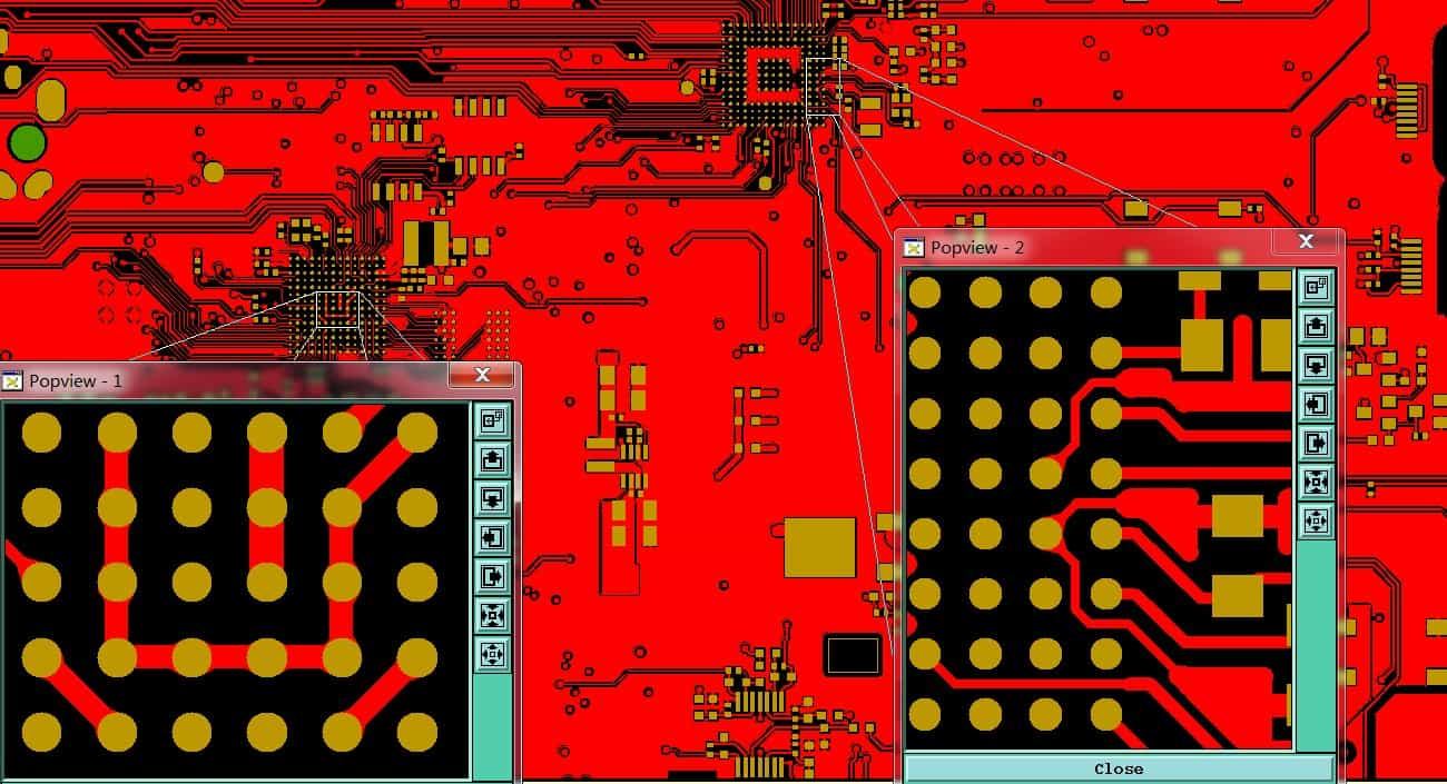
Validate Design Rules Before Manufacturing
Before proceeding with manufacturing, it is essential to validate your design to ensure its accuracy and minimize potential issues. Here are some key checks to perform using a design rule check (DRC) tool:
Connection Errors: Check for any missing or incorrect connections. Verify that all nets are properly routed and connected, and there are no open circuits or unconnected pins. This step helps ensure electrical continuity throughout the PCB.
Routing Mistakes: Look for any routing errors, such as traces that violate clearance or spacing requirements. Verify that high-speed signals are properly routed to minimize crosstalk and impedance mismatches. Check for any design rule violations related to trace width, differential pair spacing, or other routing constraints.
Outdated Silkscreen: Review the silkscreen markings on the PCB and verify their accuracy and relevance to the current design. Check for outdated or incorrect component designators, labels, or graphics. Silkscreen markings should reflect the latest component placements and revisions.
Performing these checks using a DRC tool helps identify and rectify potential design errors, improving the manufacturability and reliability of your PCB. It’s important to consult the documentation and guidelines provided by the DRC tool or the PCB design software you are using, as the specific steps and options may vary.
Additionally, consider performing other design validations, such as electrical rule checks (ERC) to catch any potential electrical issues and design reviews to ensure overall design quality and adherence to industry standards.
By validating your design rules before manufacturing, you can catch and address any errors or issues early on, reducing the risk of costly revisions or manufacturing defects.
Conclusion
In conclusion, when designing PCBs for embedded systems, it is important to consider various guidelines for PCB layout and routing, depending on the type of voltage regulator being used. Different types of regulators, such as linear regulators and switching regulators, have specific requirements to ensure optimal performance and reliability.
Additionally, incorporating thermal relief for large copper traces and pours can greatly improve the quality of soldering and help prevent the occurrence of cold solder joints.
Optimizing for surface mount technology (SMT) assembly is crucial for efficient and cost-effective production. It involves using SMT components whenever possible, leveraging SMT connectors for specific assembly requirements, and collaborating closely with the assembler when incorporating through-hole parts. These steps help streamline the assembly process and reduce associated costs.
Before proceeding with manufacturing, it is essential to validate the design rules. Tools like Design Rule Check (DRC) should be used to identify any connection errors, routing mistakes, or outdated silkscreen elements. By conducting these checks, design accuracy is ensured, and potential issues in the final product are minimized.
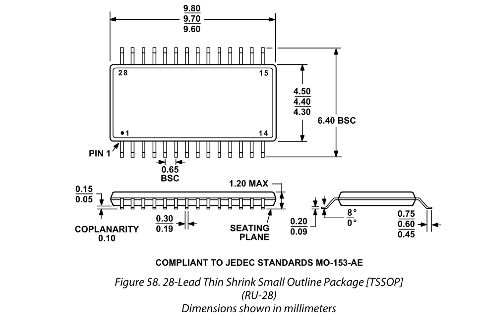
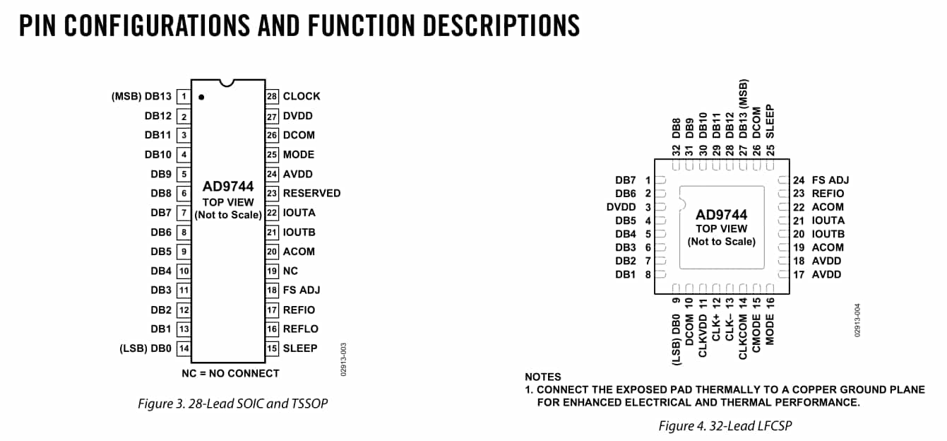
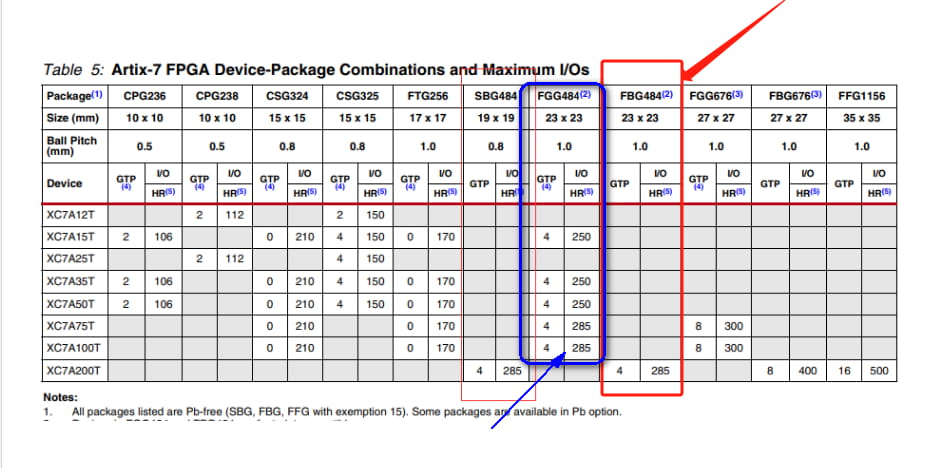
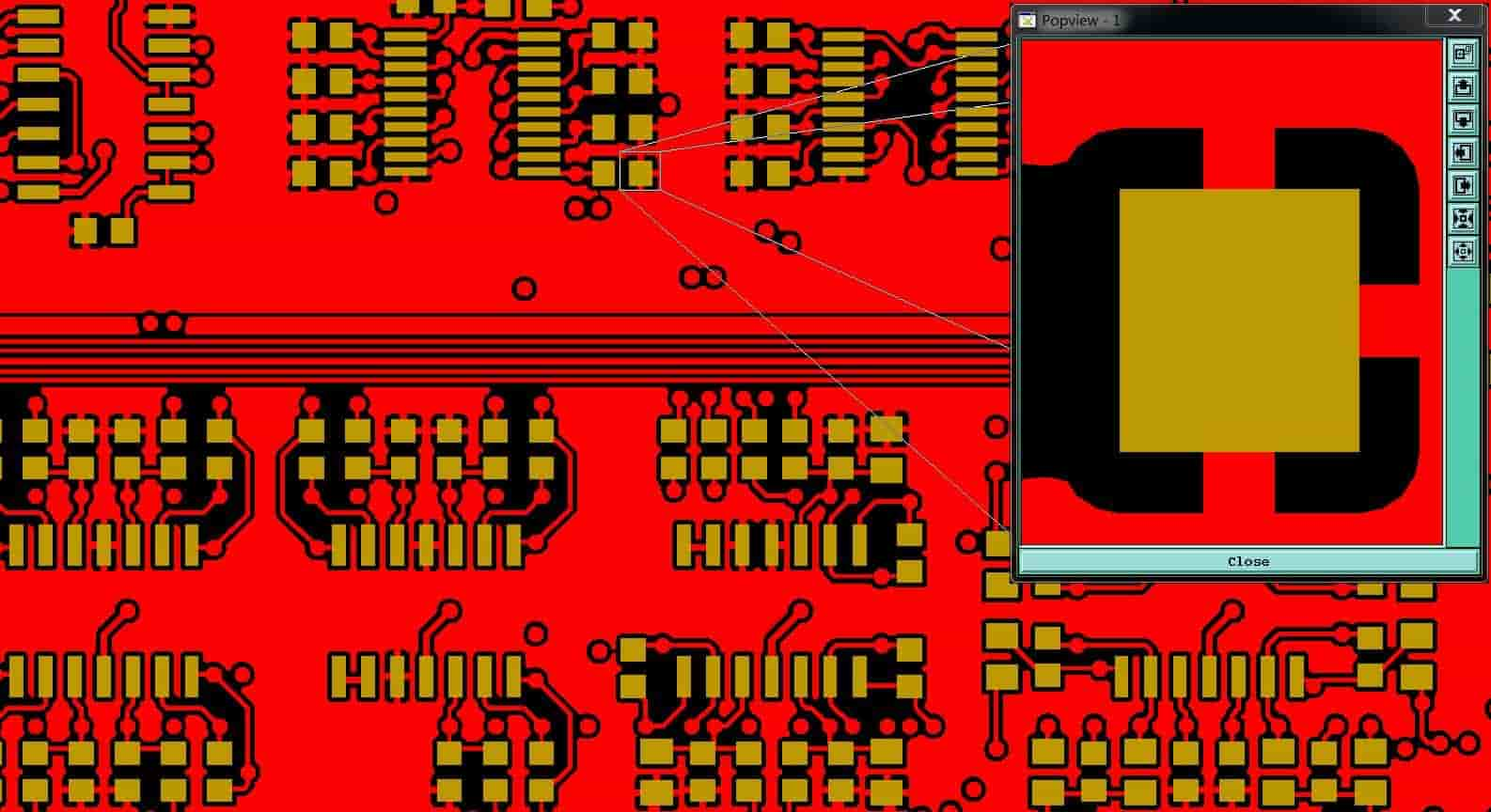
These two chips are from the same series, with similar models and different packages, so it is easy to confuse them.
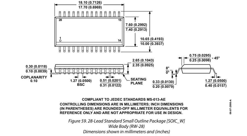
By following these guidelines and performing comprehensive design validations, you can optimize the performance, reliability, and manufacturability of your PCBs for embedded systems. Furthermore, ensuring consistency between the BOM’s package specifications and the actual Gerber solder pad dimensions is crucial for accurate component selection and smooth manufacturing processes.
Take a Quick Quote
Discover how our expertise can help with your next PCB project.