
The Ultimate Guide to Circuit Board Patterns
Introduction to Circuit Board Patterns
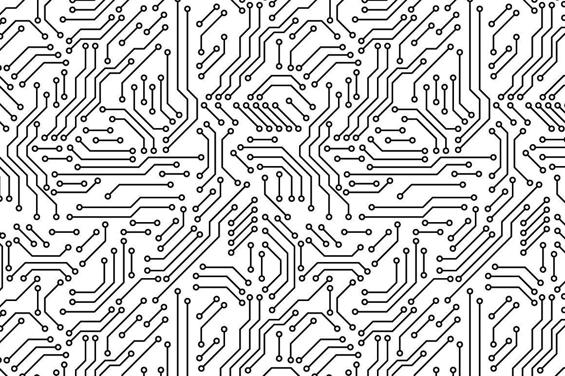
A circuit board pattern refers to the visual representation of a circuit’s layout and design. It consists of intricate configurations of lines, pads, vias, and geometric shapes that map out the arrangement of components and electrical connections on a printed circuit board (PCB).
While a circuit board pattern does not contain actual conductive materials or components, it serves as a blueprint that guides the routing of signals and power throughout the board. The pattern determines the complexity of the circuit by defining the pathways for electrical current flow between different nodes.
Properly designing circuit board patterns is crucial for establishing reliable connectivity, maintaining signal integrity, managing electromagnetic interference, distributing power, and placing components optimally. This article provides a comprehensive guide to circuit board patterns, exploring key concepts, design considerations, and applications.
PCB Pattern Design Guidelines and Considerations
Ensuring Robust Electrical Connectivity
The fundamental essence of PCB pattern design lies in its ability to ensure unwavering electrical connectivity between components. The precise placement of electronic elements and the strategic routing of conductive traces play a pivotal role in achieving this goal. In doing so, signal losses are minimized, and the reliability of the entire circuit board is significantly enhanced. This careful orchestration of the layout guarantees that signals traverse their intended paths without interruption. Furthermore, the methodical configuration of components and traces results in an electrical network that remains uninterrupted, minimizing the chances of signal attenuation and interference.
Preserving Signal Integrity
The propagation of signals through a PCB is a delicate process where preserving signal integrity is paramount. Controlled impedance routing, precise matching of trace lengths, and stringent adherence to impedance control measures act as the guardians of signal quality in this realm. They work in unison to ensure that signals maintain their integrity as they traverse the circuit. The controlled impedance routing guarantees that signals flow smoothly without suffering from distortion, while matched trace lengths are the soldiers that ensure signals reach their destination without any reflections that could impede their path. Additionally, the elimination of crosstalk ensures that the circuit operates in harmony, unburdened by signal interference.
Mitigating Electromagnetic Interference (EMI)
Electromagnetic Interference (EMI) poses a significant threat to the proper functioning of electronic devices. To shield against this menace, PCB patterns must incorporate advanced design techniques. Among these, ground planes and strategic shielding mechanisms are deployed to create a protective barrier, warding off the intrusive effects of EMI. The meticulous positioning of components is yet another tactic employed to reduce the susceptibility of the circuit to EMI. However, the ultimate safeguard lies in adhering to Electromagnetic Compatibility (EMC) standards. These standards are the bedrock of EMI mitigation, guaranteeing that the circuit functions within the allowable limits for electromagnetic interference.
Facilitating Effective Power Distribution
The foundation of proper electronic device functionality rests on the effective distribution of power. PCB pattern vectors are the architects of this operation, meticulously routing power traces to guarantee uniform power distribution with minimal voltage losses. The intricately designed power planes, along with power rails and the incorporation of decoupling techniques, form the framework of a stable power supply across the entire board. These elements ensure that power is delivered consistently to every nook and cranny of the circuit, preventing fluctuations that could undermine the reliability of the device.
Optimizing Component Placement
Strategic component placement within the PCB pattern is analogous to choreographing a precise dance for electronic elements. The act involves deftly grouping related components, ensuring proper spacing to facilitate efficient heat dissipation, and minimizing alignment lengths. This meticulous approach simplifies the process of maintenance and debugging, reduces signal propagation delays, and augments overall signal integrity. The harmonious alignment of components results in a circuit that operates seamlessly, free from any disarray that might hinder its performance.
Achieving Efficient Signal Routing
Efficient signal routing is akin to mapping out the shortest and most direct routes for the transmission of signals within the PCB pattern. Achieving this involves skillfully employing layer stacking and precise via placement to address any electromagnetic interference (EMI) issues and minimize signal coupling. Furthermore, it entails the integration of advanced routing techniques such as differential pair routing and length matching to optimize signal quality and ensure signal integrity. The choice of routing tactics is tailored to the unique demands of specific use cases, encompassing factors like trace widths, spacing, current-carrying capacity, and voltage requirements. Additionally, thicker traces are utilized for high-current paths. All these efforts coalesce to deliver a circuit with impeccable signal quality.
Designing for Manufacturability
Designing for manufacturability is an essential facet of PCB pattern design. It entails a meticulous accounting of critical parameters, including minimum trace widths, clearances, and precise pad sizes. Additionally, it demands strict adherence to design rules to guarantee an accurate assembly process and a seamless manufacturing operation. Collaboration with manufacturers in the early stages of design serves as an indispensable ally. This partnership empowers the identification and resolution of potential issues that could arise during the PCB manufacturing process. By proactively addressing these concerns, the PCB pattern is fine-tuned to align seamlessly with the manufacturing process, guaranteeing an efficient journey from design to a fully functional circuit board.
Distinguishing Between PCB Patterns and Footprints
The world of PCB design introduces us to two terms that often get used interchangeably: patterns and footprints. However, a closer examination reveals that they are distinct entities, each serving a unique purpose. Here, we delve into the detailed differences between PCB patterns and footprints, shedding light on their roles and characteristics.
PCB Pattern
The PCB pattern is the heart and soul of the circuit board, responsible for ensuring that all components are harmoniously connected. It comprises the conductive traces, pads, and vias, forming a complex network of electrical connections. These connections are crucial for facilitating the flow of signals and power between various components on the PCB.
Focus on Signal Routing and Electrical Connectivity
The primary role of the PCB pattern is to define the pathways for electrical signals. It determines how signals will travel across the board, connecting various components. The PCB pattern focuses on ensuring electrical connectivity, allowing the signals to move unimpeded. This aspect is crucial for the proper functioning of the circuit.
Ensuring Signal Integrity and EMI Control
Signal integrity and EMI control are paramount in PCB design. The PCB pattern plays a significant role in this regard by carefully routing signals and minimizing electromagnetic interference (EMI). By adhering to principles of signal integrity and EMI control, the PCB pattern guarantees that the circuit operates smoothly and without disruptions.
Determining Circuit Interconnections
The PCB pattern is responsible for defining how different components in the circuit are interconnected. It acts as a guide for the electrical connections, ensuring that each component communicates effectively with the others. Without a well-designed PCB pattern, the circuit’s functionality could be compromised.
Requires Adherence to Electrical Design Principles
To create an effective PCB pattern, designers must follow rigorous electrical design principles. These principles guide the placement and routing of conductive traces, ensuring that the circuit functions as intended. Adherence to these principles is non-negotiable for achieving a high-quality PCB pattern.
PCB Footprint
On the other hand, the PCB footprint has a different purpose and focus. It is all about the physical dimensions and layout of a component. The footprint represents the specific pads and markings on the circuit board that align with a component’s leads or pins.
Focus on Component Mounting and Soldering
The primary role of the PCB footprint is to ensure that a component can be securely mounted on the board and soldered in place. It defines the physical interface between the component and the board, allowing for a reliable mechanical and electrical connection.
Allows Accurate Placement and Orientation of Components
The PCB footprint provides the necessary information for the accurate placement and orientation of components on the board. It includes details about the size and shape of the pads, as well as any alignment markings. This ensures that components are positioned correctly during assembly.
Requires Accurate Representation of Physical Specifications
Designing a PCB footprint necessitates an accurate representation of a component’s physical specifications. This includes the dimensions of the component, the spacing between leads or pins, and any unique features that aid in placement. The precision of the footprint is crucial for successful component assembly.
In conclusion, while PCB patterns and footprints are often used interchangeably, they serve distinct purposes in the world of circuit board design. The PCB pattern focuses on electrical connectivity, signal routing, and EMI control, ensuring the circuit’s functionality. In contrast, the PCB footprint concentrates on the physical interface and placement of components, enabling secure mounting and soldering. Understanding these differences is vital for achieving a well-designed and functional PCB.
Types of Circuit Board Patterns
Several types of PCB patterns exist, each suited for different applications:
Single-Sided Patterns
Single-sided PCB patterns contain conductive traces and components on only one side of the board. The other side is blank or composed of a non-conductive material.
- Simplest and most cost-effective option
- Suitable for basic circuits with minimal complexity
- Limits design flexibility and circuit density
- Uses copper traces on a single layer for connectivity
Ideal for simple circuits like basic amplifiers, hobby electronics, and educational prototype boards.
Double-Sided Patterns
Double-sided patterns have conductive traces on both the top and bottom layers of the PCB.
- Provides increased functionality over single-sided boards
- Allows greater circuit density
- Cost-effective option for moderately complex designs
- Top and bottom layers interconnected by plated through-holes called vias
Commonly used for amplifiers, data acquisition boards, motor control circuits, and intermediate-level hobbyist projects.
Multilayer Patterns
Multilayer PCBs contain four or more alternating layers of conductive copper traces separated by insulating dielectric material.
- Accommodates highly complex and dense circuitry
- Multiple trace layers enable extensive routing capabilities
- Vias interconnect traces on different layers
- Outer layers house components and surface traces
- Inner layers contain signal routing traces
- More expensive to fabricate than single or double-sided
Ideal for complex digital circuits, processors, telecommunication devices, military equipment, and other advanced electronics.
Power Plane Patterns
Power planes provide entire board layers dedicated to distributing power.
- Comprised of large copper regions that act as power supply rails
- Provide low-impedance distribution networks for each power source
- Enhance signal integrity by minimizing power supply noise
- Improve thermal performance by spreading heat
- Essential for high-speed digital logic and analog circuits
Ground Plane Patterns
Ground planes dedicate entire board layers for ground distribution.
- Large copper regions act as low-impedance ground nodes
- Provide uniform ground reference for return currents
- Shield signals from EMI interference
- Enhance signal integrity and reduce noise
- Often incorporated with power planes in multilayer boards
Differential Pair Patterns
Differential pairs route two traces in parallel while carrying equal and opposite signals.
- Achieve precise timing and maximize noise immunity
- Carefully controlled trace dimensions, spacing, and impedance
- Common in high-speed analog and digital applications
- Used in systems where signal quality is paramount
Clock Distribution Patterns
Distribute clock signals from a common source to multiple destinations.
- Provide synchronized timing to various circuit blocks
- Ensure clock signals arrive simultaneously to all clocked components
- Eliminate skew between system elements
- Often designed as tree structures or grids
Essential for microprocessor and high-speed digital systems requiring precise timing.
RF Transmission Line Patterns
Designed to properly route high-frequency RF and microwave signals.
- Incorporate impedance-matched transmission lines
- Enable efficient transfer of signals from source to load
- Prevent unwanted reflections that corrupt signal integrity
- Aid in circuit tuning by controlling inductance and capacitance
Vital for RF circuits in radar systems, communications, cellular networks, and other wireless applications.
The Essential Functions of PCB Patterns
PCB patterns play a crucial role in the world of circuit board design. They are the intricate frameworks that ensure a circuit board’s functionality. Let’s dive into the detailed functions and significance of PCB patterns:
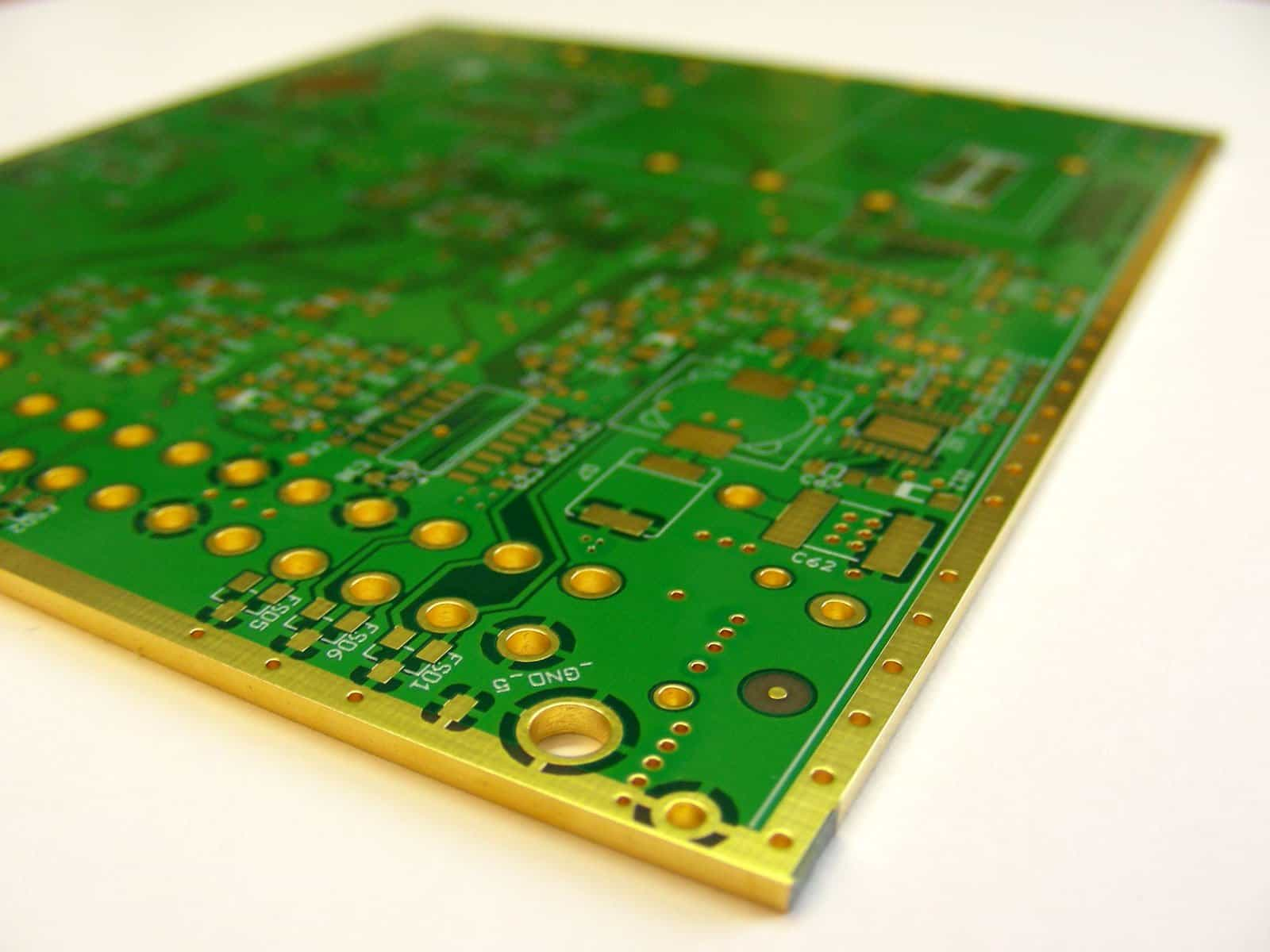
Creating Conductive Traces
At the heart of every PCB pattern are conductive traces. These traces are etched onto copper sheeting, forming complex pathways for electrical signals to travel. Much like the wires in a traditional electrical system, these traces carry currents, allowing for the seamless interconnection of components across the circuit board.
Providing Pads for Components
Components such as resistors, capacitors, and integrated circuits have leads or pins that require secure attachment to the circuit board. PCB patterns expose selected copper regions as pads. These pads serve as the designated areas for soldering component leads, establishing both mechanical and electrical connections. The accuracy and reliability of these soldered connections are critical to the circuit’s overall performance.
Enabling Connections Through Vias
For multilayer PCBs, where multiple layers of conductive traces are used to accommodate complex circuits, vias play a pivotal role. Vias are drilled holes in the board that are plated with conductive materials. They create pathways for signals to pass between different layers of the circuit board. These interlayer connections enable intricate routing of signals and ensure that the various components can communicate effectively.
Establishing Electrical Connectivity
One of the primary functions of PCB patterns is to establish electrical connectivity. The network of conductive traces acts as an interconnected system, facilitating the transmission of electrical signals between components. This web of connections ensures that the entire circuit operates as a unified entity. Without proper electrical connectivity, the circuit’s functionality would be severely compromised.
Defining Signal Pathways
Signal integrity is paramount in PCB design. The careful routing of traces in the pattern is instrumental in maintaining the integrity of electrical signals. Each trace is responsible for directing signals along their intended paths, ensuring they reach their designated destinations without distortion or interference. By meticulously planning and designing these pathways, PCB patterns contribute to the reliability and performance of the circuit.
Distributing Power
Power distribution is a critical aspect of any electronic device’s functionality. PCB patterns address this need by incorporating power and ground planes into the design. These planes create stable and noise-free pathways for power distribution. By ensuring uniform power distribution across the board, PCB patterns minimize voltage variations and contribute to the overall stability and efficiency of the circuit.
In summary, PCB patterns serve as the backbone of circuit board design, performing several indispensable functions. They create conductive traces, provide pads for component attachment, enable multilayer connections through vias, establish electrical connectivity, define signal pathways for signal integrity, and ensure efficient power distribution. These patterns are the intricate blueprints that make complex electronic systems possible.
Applications of PCB Patterns in Telecom and Networking
In the realm of telecommunications and networking, where speed, precision, and reliability are paramount, advanced PCB patterns are essential. Let’s explore how PCB patterns are tailored to meet the unique demands of these critical industries:
Power Distribution and Grounding
Effective power distribution and grounding are crucial in networking and telecommunications applications. Board patterns that incorporate power and ground planes ensure stable power supply and reliable grounding. Power planes provide low-impedance paths for uniform power distribution, minimizing voltage losses and ensuring consistent power supply to different components. Proper grounding reduces noise and enhances the overall performance of the system.
Multilayer PCB Designs
The complexity of networking and telecommunications systems often demands the use of multilayer PCB patterns. These patterns consist of multiple layers of conductive traces and insulating materials, catering to high-density circuit requirements. The additional layers in these patterns are essential for proper signal routing, efficient power distribution, and the isolation of sensitive analog and digital signals. By doing so, they significantly reduce noise coupling and interference, ensuring that data flows without hiccups in these intricate systems.
Signal Routing and Switching
Telecommunication and networking systems are complex ecosystems where data flows between various components, devices, and network nodes. The PCB pattern is the enabler of efficient signal routing and switching within these systems. As the PCB pattern is designed, critical factors such as noise coupling, signal timing, and cross-talk are considered. This meticulous planning ensures that signal switching and routing are accurate and dependable. In a world where seamless data transfer is non-negotiable, PCB patterns play a pivotal role in keeping the information flowing.
RF and Microwave Applications
Wireless networks and telecommunication systems are heavily reliant on radio frequency (RF) and microwave technologies. To meet the specific needs of these applications, PCB patterns are meticulously optimized. These patterns feature impedance-matched transmission lines, ground plane structures, and specialized RF protection systems. This level of detail is essential to ensure that signals move effectively, with minimal signal reflections and a firm grip on controlling EMI interference. By enhancing signal quality and system performance, PCB patterns become a key player in ensuring that wireless communication remains swift, interference-free, and reliable.
High-Speed Signal Transmission
In the world of networking and telecommunications, high-speed data transmission is the lifeblood that keeps the systems running. This necessitates a high-quality signal flow that is error-free. To achieve this, the design of the PCB pattern takes into account several critical factors. These include the prevention of signal degradation, mitigation of electromagnetic interference (EMI), and minimization of signal losses. The PCB pattern ensures that signals are transmitted correctly and reliably, even over extended distances with high data rates. It accomplishes this by employing controlled impedance transmission lines and reducing parasitic capacitance and inductance. The result is a PCB pattern that acts as a guardian of data integrity, guaranteeing the seamless and swift transmission of critical information.
Conclusion
In conclusion, circuit board patterns play a vital role in PCB design, serving as the blueprint for the layout, connectivity, and functionality of electronic circuits. By following the key design guidelines and considerations, designers can ensure proper electrical connectivity, maintain signal integrity, control electromagnetic interference (EMI), enable effective power distribution, optimize component placement, achieve efficient signal routing, design for manufacturability, and incorporate thermal management.
Highleap is a leading PCB and PCBA manufacturer that can assist in implementing these guidelines and considerations. With their expertise and collaboration, designers can create robust and reliable circuit board patterns that meet the specific requirements of their projects. By leveraging Highleap’s capabilities and knowledge, designers can enhance the performance, reliability, and manufacturability of their PCB designs.
Whether it’s ensuring proper electrical connectivity, managing signal integrity, controlling EMI, optimizing power distribution, or incorporating thermal management, Highleap can provide the necessary expertise and support throughout the PCB design process. Their collaboration can help designers overcome challenges and achieve successful outcomes in their PCB projects.
Take a Quick Quote
Discover how our expertise can help with your next PCB project.