
Back to blog
How to Design Power PCB?

Power PCB Design
Power supplies are the backbone of modern electronics, providing the necessary voltage and current to various circuits and devices. Whether you are designing a power supply for a small electronic gadget or a complex industrial application, there are several key considerations to ensure optimal performance, reliability, and efficiency. In this comprehensive guide, we will delve into the intricate details of designing a power PCB, covering various aspects from topology selection to thermal management and compliance testing.
Power PCB Functional Requirements
Before diving into the technical aspects of power PCB design, it’s crucial to establish the functional requirements. These requirements serve as the foundation for the entire design process. Consider the following factors:
- Input Voltage Range: Define the expected input voltage range, including minimum, nominal, and maximum voltages. This range is critical for designing a power PCB that can maintain regulation under varying conditions.
- Output Voltages and Currents: Specify the desired output voltages and load currents. Take into account any multiple outputs, cross-load dependencies, and sequencing requirements.
- Efficiency Targets: Set efficiency targets for full load and partial load conditions. Efficient power conversion is essential for reducing energy consumption and heat generation.
- Power Density Targets: Determine the desired power density, which influences the physical size and packaging of the power supply. Balancing power density with efficiency and thermal performance is crucial.
- Safety and Emissions Compliance: Consider regulatory standards such as safety certifications (e.g., UL, CSA), conducted emissions, and radiated emissions compliance. Ensure that your design meets these standards.
- Reliability Requirements: Define reliability metrics, including Mean Time Between Failures (MTBF), expected service life, and environmental survivability. These metrics guide component selection and redundancy considerations.
- Control Characteristics: If your application requires remote control, sequencing, telemetry, or margining control, specify these needs to integrate advanced control features.
Topology Selection
Selecting the appropriate power conversion topology is a critical decision in power supply design. Different topologies have distinct advantages and limitations. Here are some common options:
- Linear Regulator: Linear regulators are simple and provide low-noise output. They are suitable for low-power applications but are less efficient and generate more heat.
- Switching Regulator: Switching regulators are highly efficient and can handle higher input voltages. They are ideal for high-power applications but may generate more electromagnetic noise.
- Buck Converters: Used for step-down voltage conversion.
- Boost Converters: Used for step-up voltage conversion.
- Buck-Boost Converters: Allow both step-down and step-up conversion.
- Isolated Topologies: Flyback, forward, push-pull, and full-bridge converters use transformers for isolation and multiple outputs.
The choice of topology depends on factors like required conversion ratio, complexity, component stresses, efficiency goals, and isolation needs. Careful consideration is essential to meet your specific application requirements.

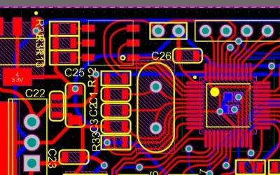
Power PCB-Inverter DC boost board
Power Stage Design
The power stage of a power supply handles the actual power conversion between input and output. It consists of various components, including switches, diodes, inductors, transformers, and capacitors. Here are key aspects to consider:
- Semiconductor Switch Selection: Choose between MOSFETs and IGBTs based on your power supply’s wattage requirements. High-current MOSFETs simplify synchronous rectifier buck designs, while IGBTs are more robust for high-power applications.
- Passive Components:
- Inductors: Select inductor values to balance ripple, response time, and component size. Core materials and shapes impact efficiency.
- Transformers: Consider core geometry, materials, gap design, winding techniques, and layering for optimal performance.
- Capacitors: Use a mix of electrolytic and multilayer ceramic capacitors for bulk capacitance and high-frequency bypassing.
- Snubbers and Clamps: Implement snubbers like RC networks to suppress voltage spikes across switches during transitions. Clamps help limit overvoltage events.
- Layout and Parasitics: Carefully place components and route traces to minimize high-current paths’ length, reducing parasitic inductance and resistance. Isolate noisy switching nodes from sensitive analog areas.
Feedback and Control in Power PCB Design
Maintaining stable regulated output voltages is critical in power PCB design. Feedback control forms a closed-loop system that adjusts PWM switching patterns based on output voltage deviations from the reference. Consider these aspects:
- Voltage Dividers: Design resistive divider networks to scale output voltages to levels acceptable for the feedback IC. Add filtering for noise reduction.
- Feedback IC: Utilize specialized ICs that provide operational amplifiers, PWM control, compensation circuits, and protection features necessary for robust control and regulation.
- Compensation Network: Create a compensation network to ensure stable control loop operation. Set gain crossover and phase margin to achieve stable response with noise immunity.
- Digital Control: Incorporate digital control for advanced features such as monitoring, diagnostics, communication, and adaptive tuning. This allows for sophisticated control algorithms and remote user interfaces.
- Protection Features: Implement essential protection features to safeguard the power PCB and connected load during abnormal conditions. Common protections include overvoltage, undervoltage, overcurrent, over-temperature, and input voltage lockout.
Thermal Management
Effective thermal management is crucial to ensure reliable operation and safety in power supplies. Consider the following aspects:
- Power Dissipation Analysis: Analyze power dissipation in switches, magnetics, and other components to determine cooling requirements. Use analytical methods and simulations for validation.
- Heatsink Design: Design heatsinks to provide convective cooling. Optimize fin geometry, airflow passages, heat pipe usage, and interface materials for efficient heat dissipation.
- Airflow and Ventilation: Use fans and airflow ducting to maintain directed airflow through heatsinks and enclosures. Intake and exhaust vents should be designed for natural convection as well.
- Thermal Interface Materials (TIMs): Choose appropriate TIMs such as thermal pads, greases, or phase-change compounds to enhance heat conduction from components to heatsinks.

Highleap Electronic – Power PCB Design
EMI/EMC Design Considerations for Power PCBs
Switching power supplies generate high-frequency electromagnetic noise, which must be mitigated to comply with EMI (Electromagnetic Interference) limits and prevent device interference. Key design aspects include:
- Input Filtering: Utilize pi-filters and ferrite beads to suppress differential mode noise from the AC input.
- Output Filtering: Employ capacitors, ferrites, and LC filters to clean DC output noise and protect downstream circuits.
- Circuit Partitioning: Physically separate noisy power circuits from sensitive analog and digital areas using partitioning, shielding, and isolation techniques.
Techniques for EMI Reduction
To minimize emissions at the source, explore spread spectrum frequency modulation, soft-switching, snubbers, proper grounding, and shielding. Ensure proper enclosure shielding and correct installation of filter feedthrough components to contain radiated emissions. Power PCB stitching vias can help shield leakage from ground plane gaps, further enhancing EMI control.
Physical Design and Packaging Considerations for Power PCBs
Designing the physical aspects of a power supply isn’t just about functionality—it’s about ensuring the product is user-friendly, safe, and reliable. The enclosure provides crucial support and safety isolation, while also managing EMI shielding and airflow to keep components cool. A well-thought-out Power PCB layout minimizes high-current paths and reduces noise, making the device easier to service and manufacture.
Reliable connections to external interfaces and clear operational indicators are vital. Environmental protection, such as conformal coatings and potted enclosures, shields the Power PCB from dust, moisture, and vibrations, ensuring long-term durability and performance.
Compliance Testing and Certifications
Verification testing and certifications are essential to ensure that your power supply design meets regulatory and safety standards. Here are key testing areas:
- Functional Testing: Confirm basic functionality under various operating conditions, including load variations, voltage changes, temperature extremes, and frequency shifts. Burn-in reliability testing can also be conducted to stress components.
- Safety Standards: Seek certifications from relevant authorities (e.g., UL, CSA, ENEC) to meet end-use product safety requirements, including insulation, fault tolerance, construction, and marking.
- EMI and EMC Testing: Conduct testing for conducted and radiated emissions, immunity to interference, and surge withstand to verify compliance with FCC, CE, and other standards.
- Environmental Tests: Ensure that the power supply can operate under challenging environmental conditions, including temperature, humidity, vibration, shock, salt-fog, and ingress protection.
Conclusion
Designing a PCB power supply is a multifaceted process that demands expertise in various engineering domains, including power electronics, analog design, thermal management, and compliance testing. A structured approach, guided by functional requirements, topology selection, and meticulous component choices, is essential to create a reliable and efficient power supply tailored to your application’s needs.
The demand for well-designed, cost-effective power supplies continues to grow as electronics become increasingly integral to our daily lives. By following the principles outlined in this comprehensive guide, electrical engineers can navigate the complexities of power supply design and deliver solutions that meet the highest standards of performance, reliability, and safety.

Related Articles
Analysis of Power Supply Noise in HF PCB Design Process
This comprehensive guide explores the complexities of power supply noise, its origins, and advanced techniques to mitigate its effects in high-frequency PCB designs.
What is EMI, EMS and EMC?
At Highleap Electronic, we specialize in producing high-quality PCBs by integrating advanced techniques for impedance control, ensuring robust EMC and mitigating EMI.

Boosting PCB Manufacturing Efficiency with Laser Direct Imaging (LDI)
LDI achieves sub-micron resolution and precise control over line widths, critical for manufacturing high-density interconnect boards and fine-pitch components.
Take a Quick Quote