
Back to blog
Multilayer PCB Benefits and Applications
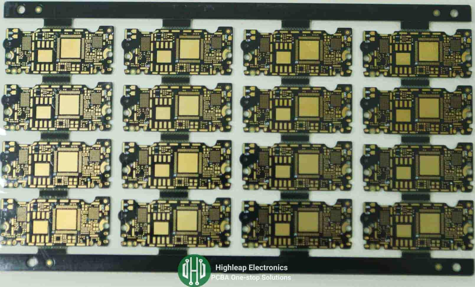
Introduction to Multilayer PCB Technology
Printed circuit boards (PCBs) play a vital role in virtually all electronic devices by providing the platform for integrated circuits and other electronic components to interconnect. As circuit complexity increased over the decades, single and double layer PCBs could no longer meet the density and performance requirements of modern electronics. This necessitated the development of multilayer PCB technology which enables significantly higher component packing by utilizing multiple insulating and conductive layers in a single board.
Today, multilayer PCBs have become ubiquitous across various industries due to their key advantages over single/double layer boards including smaller form factors, greater routing flexibility, improved signal integrity, increased reliability and lower costs over multiple boards. This article aims to provide a comprehensive overview of multilayer PCB technology – exploring the key concepts, manufacturing processes, design considerations, applications and latest trends.
Types of Multilayer Printed Circuit Boards
The types of multilayer printed circuit boards (PCBs) can be broadly categorized into three main types, each with unique characteristics and applications:
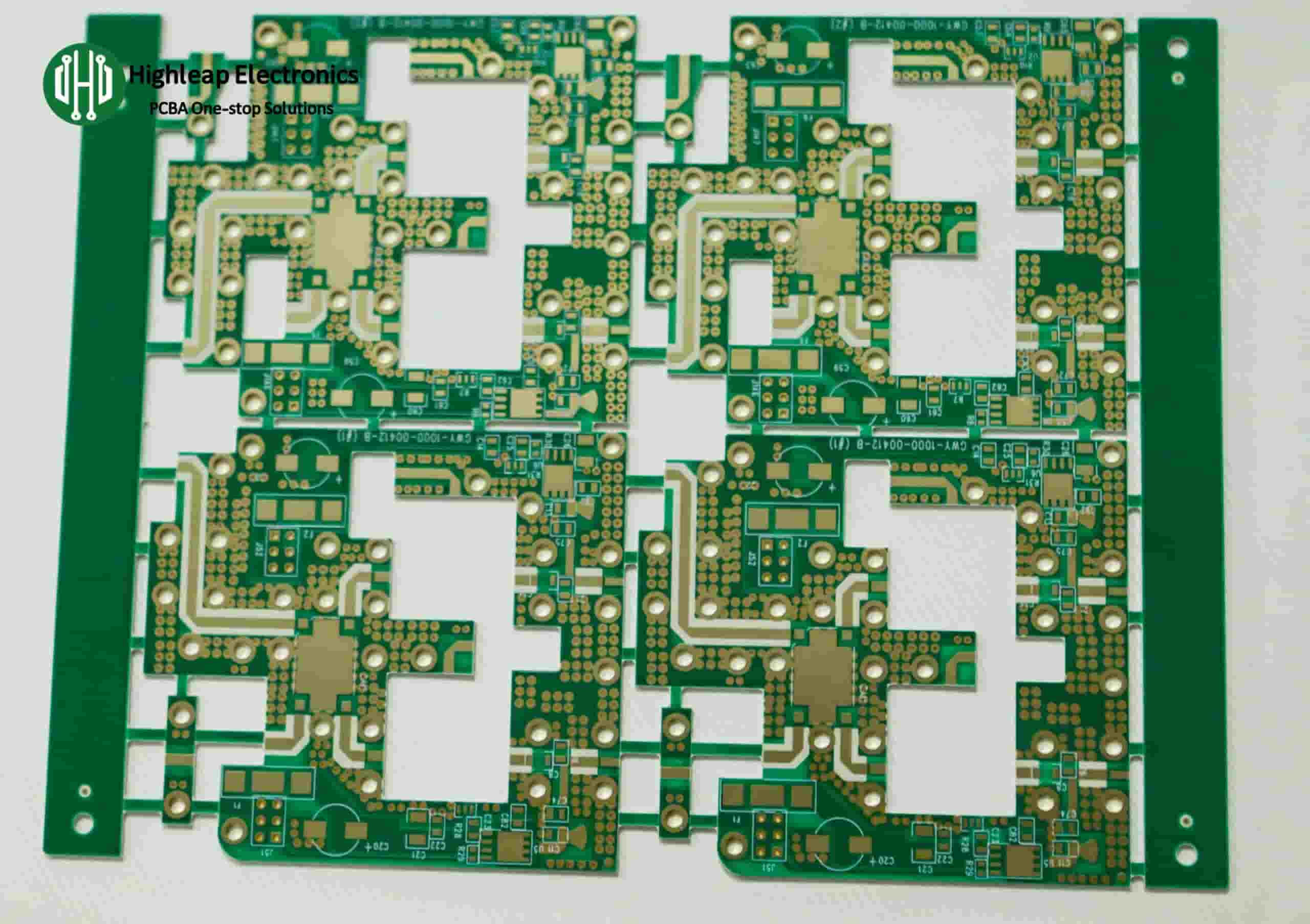
- Rigid Multilayer PCBs:
- Definition: These PCBs are inflexible and cannot be bent or twisted. Their rigidity is due to the use of an FR4 stiffener or similar rigid substrate material.
- Characteristics: They maintain their shape after installation and are known for their strength and durability. Rigid multilayer PCBs can have more than 12 layers.
- Applications: Commonly used in electronic devices where the PCB shape is static and longevity is important. Examples include motherboards in computers, where they house components like RAM, GPU, and CPU.
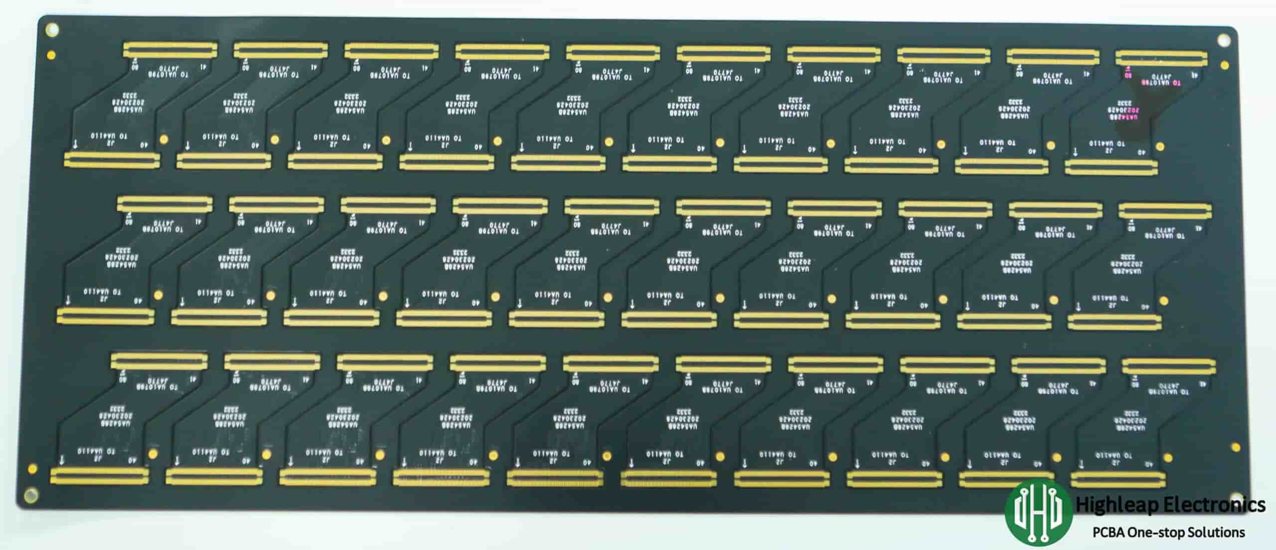
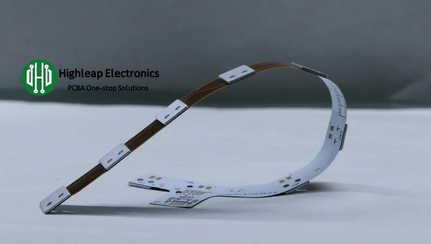
- Flex Multilayer PCBs:
- Definition: These are flexible circuits that can have three or more conductive layers. They are built by combining single or double-sided circuits using advanced connection and shielding techniques.
- Flexibility: While they offer flexibility, the level of flexibility can vary depending on the lamination process. Continuous lamination can increase rigidity with each added layer.
- Benefits: They are lighter and can reduce package size, thanks to thin dielectric substrates. Advantages include reduced assembly errors, design freedom, improved airflow, and increased heat dissipation.
- Applications: Ideal for high-density applications where space and weight are critical, such as in aerospace technology.
- Rigid-Flex Multilayer PCBs:
- Definition: A hybrid type that combines the features of both rigid and flexible PCBs. It consists of rigid multilayer circuit boards connected to flexible circuit boards.
- Characteristics: This design offers the strength of rigid PCBs and the flexibility of flex PCBs, optimizing the space occupied by the board. However, increasing the number of layers in the flexible section can reduce its flexibility.
- Applications: Widely used in applications where space, weight, and performance are crucial. Aerospace is a notable industry that utilizes rigid-flex PCBs for their space-saving and lightweight properties.
Each of these PCB types is engineered to meet specific requirements in electronic design, offering solutions for various challenges in modern electronics, such as miniaturization, durability, and complex circuitry management.
Advantages of Multilayer PCB Technology
The advantages of multilayer PCB technology, contributing to its widespread adoption across various industries, include:
Smaller Form Factor: Multilayer PCBs consolidate multiple circuit board functions into a single, compact board, reducing the overall size of electronic devices.
Increased Component Density: These PCBs allow mounting more components per unit area, thanks to inner conductive layers and interlayer vias, enabling complex circuits in limited spaces.
Improved Electrical Performance: Offering dedicated planes for signals, power, and ground, multilayer PCBs enhance noise isolation, controlled impedance routing, and reduce electromagnetic interference.
Enhanced Thermal Management: Plane layers in these PCBs can be patterned to effectively direct heat away from critical areas, improving heat dissipation.
Higher Reliability: The strong bonding between laminated layers in multilayer PCBs provides better resistance to temperature fluctuations, vibrations, moisture, and mechanical stress.
Ease of Assembly/Testing: Integrating several simpler boards into one multilayer board simplifies the assembly and testing processes.
Lower Overall Cost: Substituting multi-board solutions with a single multilayer board can reduce material, labor, and inventory costs.
Design Flexibility: Multilayer PCBs allow for easier last-minute modifications by re-routing on inner layers, offering more flexibility compared to single or double-layer boards.
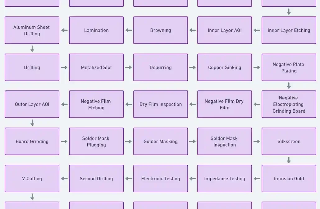
Evolution of Multilayer PCB Manufacturing Processes
The core processes involved in fabricating multilayer PCBs have notably evolved over the decades to enable higher layer counts, finer feature resolutions, tighter dimensional tolerances and via fill requirements – all while improving manufacturing yields and reducing per-board costs. Some of the key manufacturing developments include:
- Emergence of Laser Direct Imaging (LDI) technology: Replaced older photographically-based film imaging to enable higher resolutions below 10 microns as needed for high-density designs.
- Introduction of semi-additive plating: Complemented subtractive plating by selectively depositing copper only where needed, improving manufacturability of buried and blind microvias.
- Development of aqueous dry film resists: Improved overall exposure and development quality compared to previous solvent-based resins.
- Implementation of stacked via-in-pad designs: Enabled higher microvia aspect ratios by integrating full via fills within panelized pad structures.
- Transition to full-panel processing: Moved away from drilling/plating individual boards to processing whole uncut panels, improving yields for Methyl etch and Via-in-pad designs.
- Advancements in laser drilling: Transitioned from mechanical drilling to pulsed laser sources for improved accuracy, taper control and buried microvia formation in the 5-15 micron range.
- Development of in-process inspection capabilities: Integrated AOI, x-ray and other techniques for real-time defect detection to improve yields of complicated via structures.
- Implementation of innerlayer laser processing: Improved layer-to-layer registration accuracy to less than 2 microns by selectively ablating or modifying inner layers.
- Widespread use of build-up technology: Enables fabricating boards from the substrate outwards for manufacturing rigid-flex and other complex multi-material designs with higher layer counts.
Multilayer PCB Design Process and Considerations
Effective design is critical to fully leverage the capabilities of multilayer PCB technology while ensuring manufacturability, reliability and adherence to design rules. Here are some of the key aspects of multilayer PCB design:
Schematic Creation: Use EDA tools to design schematics and define component nets before layout.
Board Stackup Planning: Select number of layers, layer types (signal, power, ground) and layer thicknesses based on design requirements.
Footprint Creation: Define footprint libraries with drill sizes/shapes, pad sizes suited for surface mount/through-hole components.
Component Placement: Strategy components on board areas while following assembly and thermal guidelines.
Inner Layer Routing: Route signal and reference planes within layer stackup to isolate noise and manage impedance.
Via Placement: Strategically place blind/buried/stacked vias to optimize routing density without compromising manufacturability.
Outer Layer Routing: Route components to pads/vias on outer layers taking assembly/testing access into account.
Design Rules Checking: Verify compliance to stackup, spacing, width and electrical connectivity rules.
Gerber File Creation: Output design data in standardized Gerber format for fabrication.
Electromagnetic Simulation: Simulate and validate signal integrity, power integrity, EMI/EMC performance before fabrication.
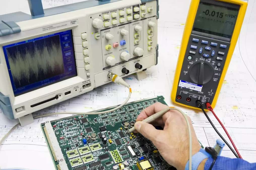
Prototype Manufacturing/Testing: Iterate design based on prototype results to ensure design goals are met.
Key Materials Used in Multilayer PCB Fabrication
In the fabrication of multilayer printed circuit boards (PCBs), a variety of specialized materials are employed, each selected for its unique properties that contribute to the PCB’s performance, durability, and manufacturability. A detailed overview of these materials is as follows:
Base Material/Substrate:
- FR-4 Glass-Reinforced Epoxy Laminate: This is the most commonly used substrate in PCB manufacturing. FR-4 is favored for its excellent balance between electrical insulation properties, mechanical strength, thermal resistance, and cost-effectiveness. It consists of woven fiberglass cloth with an epoxy resin binder.
- Alternative Substrates: Other materials like Polyimide, BT-Epoxy, and Ceramic substrates are also used. Polyimide offers higher thermal stability and flexibility, making it suitable for high-temperature applications or flexible PCBs. BT-Epoxy provides better moisture resistance and is used in high-frequency applications. Ceramic substrates are chosen for their superior high-temperature handling and thermal conductivity, beneficial in LED and high-power applications.
Conductive Material:
- Copper: Copper is the primary choice for the conductive traces on PCBs due to its excellent electrical conductivity, thermal properties, and ease of etching during the manufacturing process. Copper layers are typically added to the substrate in varying thicknesses, depending on the current-carrying requirements of the PCB.
- Aluminum and Other Metals: In certain high-power or thermal management applications, metals like Aluminum are used. Aluminum-backed PCBs are common in LED lighting and power electronics, where heat dissipation is a critical factor.
Dielectric Material:
- Epoxy Resin Systems: These systems, often based on the same material as the FR-4 substrate, are used as dielectric layers in multilayer PCBs. These layers provide electrical insulation between the different conductive planes, preventing short circuits and preserving signal integrity. The dielectric constant, loss tangent, and thermal properties of these materials are crucial in high-speed and high-frequency PCB applications.
Solder Mask:
- Liquid Photoimageable Solder Mask (LPSM): This is a commonly used type of solder mask in PCB manufacturing. It is applied to the PCB in a liquid form and then cured and developed to form a solid protective layer over the copper traces. LPSM helps prevent solder bridging during component soldering and protects the copper from environmental factors.
- Dry Film Photoimageable Solder Mask: Used in applications where precision and fine-line features are required. It is applied as a dry film and processed similarly to LPSM, providing a high-resolution protective layer.
Legend Materials:
- Ink for Component Markings: This ink is used to print legends, component identifiers, and other markings on the PCB. Typically, a polymer thick film ink is used for its durability and the ability to maintain legibility under various environmental conditions. The ink is cured to ensure it adheres firmly to the PCB surface.
Finish Materials:
- Surface Finishes: These are applied to the exposed copper areas of a PCB to protect them from oxidation and to provide a solderable surface. Common types include:
- Hot Air Solder Leveling (HASL): Involves coating the PCB with molten solder and then leveling it with hot air knives.
- Electroless Nickel Immersion Gold (ENIG): Provides a flat surface and is widely used for its good solderability and wire bonding characteristics.
- Organic Solderability Preservatives (OSP): A water-based, organic surface finish that provides a temporary protection to the copper surfaces.
Each of these materials is selected based on the specific requirements of the PCB, such as electrical performance, thermal management, manufacturing process, and the intended application environment. The choice and combination of these materials significantly influence the quality, performance, and lifespan of the multilayer PCB.
Multilayer PCB Design Tips
Designing a multilayer PCB requires careful planning and consideration to ensure functionality, manufacturability, and reliability. Here are some detailed tips and considerations for designing multilayer PCBs:
Optimize the Board Size:
- Determine the optimal board size by considering the number and size of components, the intended location for the board, and the manufacturer’s specifications for spacing, clearances, and drill holes.
- This step is crucial in balancing the design’s physical constraints with its functional requirements.
Layer Design Optimization:
- Design the layers based on the types of signals (digital, analog, RF, etc.).
- Consider the pin density and the need for controlled impedance when determining the number of layers.
- Ensure that the signal integrity is maintained by strategically placing signal, power, and ground layers.
Via Selection:
- Choose the right type of vias (through-hole, blind, buried, or via-in-pad) based on your design’s complexity and functionality.
- Each via type has its implications on the manufacturing process and PCB performance.
Material Selection:
- Select materials for each layer that meet your functional requirements. Common materials include FR-4 for general use, Polyimide for high-temperature applications, and Rogers materials for high-frequency designs.
- Ensure that the distribution of signal layers and plane layers is symmetrical to prevent issues like warping or twisting.
Manufacturing Considerations:
- Choose a reputable contract manufacturer that can meet your design specifications.
- Consider factors such as accuracy, quality control, and adherence to DFM (Design for Manufacturability) guidelines.
- Select appropriate solder masking options and trace parameters that align with your design’s needs.
Component Sourcing:
- When sourcing for components, consider factors like the function fit, availability, quality, price, and manufacturer’s credibility.
- Use a detailed Bill of Materials (BOM) that specifies the required components and materials, including their specifications, footprints, and part numbers.
- Evaluate supplier reliability, shipping costs, warranty terms, technological advancement, and experience.
- Review customer feedback, but remember to cross-check these reviews with other attributes for a balanced view.
By adhering to these design tips and considerations, you can create a multilayer PCB that is both efficient in performance and feasible in manufacturing, avoiding common pitfalls such as imbalanced load during pressing or issues with layer thicknesses that can lead to board warping or twisting.
Multilayer PCB Design Process
Designing a multilayer printed circuit board (PCB) involves a detailed and methodical process. This process requires attention to various technical aspects to ensure the final product meets all functional and quality requirements. Here’s an expanded explanation of the multilayer PCB design process:
1. Pre-design Considerations:
- Negative Plane Layers: These are critical for creating power and ground planes. Ensure appropriate clearance around pad footprints to avoid shorts.
- Pad Shapes: Different pad shapes may be needed for inner and outer layers. Customize your PCB library to accommodate these variations.
- Design Adaptations: Adapt logos, tables, and views to suit multilayer board requirements.
2. Software Selection for PCB Design:
- Choose a suitable PCB design software like KiCad, ORCAD, Eagle, or Altium Designer, based on your specific needs and comfort level.
- These software tools offer functionalities to create schematics, design board layouts, and generate necessary output files for manufacturing.
3. Schematic Diagram Creation (Using KiCad as an Example):
- Eeschema Module: Start by creating the electrical schematic using KiCad’s Eeschema. This involves selecting and placing component symbols and connecting them to form the circuit.
- Component Association and Netlist Generation: Assign footprints to the schematic symbols and generate a netlist, which is a data file that describes the connections between the components.
- Initial Steps: Begin with defining the number of layers and their specific purposes (signal, power, ground) in the ‘Layers Setup’.
- Component Placement and Routing: Place the components on the board and route the connections based on the netlist. Pay attention to signal integrity, thermal management, and mechanical constraints.
- Via Selection: Decide on the types of vias (through-hole, blind, buried) based on the interconnection needs between different layers.
- Run a DRC to identify any issues with spacing, trace widths, and other parameters that could affect the manufacturability of the board.
6. Output File Generation:
- Generate Gerber files and other necessary manufacturing output files.
7. Prototyping Process:
- Prototype Design: Follow the outlined PCB design to create a prototype, allowing for testing and validation.
- Component Sourcing: Use the Bill of Materials (BOM) to source all necessary components.
- Route Designing: Design the PCB routes considering power levels and noise sensitivity.
8. Prototype Fabrication and Assembly:
- Fabrication: Print inner layers, laminate layers, drill holes, and plate with copper.
- Assembly: Apply solder paste, place components (SMD and through-hole), and proceed with reflow soldering. Conduct inspections and functionality testing.
9. Multilayer PCB Fabrication (For Final Product):
- Core Preparation and Layering: Prepare the inner core and apply layers of copper foil and prepreg. Use dry-film resist for imaging and develop the layer patterns.
- Drilling and Plating: Drill vias and plate them for conductivity.
- Outer Layer Processing: Apply the outer layer resist, develop the pattern, and etch away excess copper.
- Finishing Touches: Apply solder mask, surface finish, and silkscreen for labels.
- Cutting and Inspection: Route or score the PCB to size and conduct final electrical and visual inspection.
10. Packaging and Shipment:
- Package the finished boards carefully and prepare them for shipment to the client or assembly facility.
Throughout this process, it is essential to maintain close coordination with the fabrication and assembly teams to ensure the design is manufacturable and meets all functional requirements. Regular checks, both electronically and physically, are crucial at each stage to identify and rectify any issues early in the process.
Uses of Multilayer Printed Circuit Boards
The advantages of multilayer PCBs have indeed made them highly suitable for various industries and applications. Here are some specific uses of multilayer printed circuit boards:
Consumer Electronics: Multilayer PCBs are extensively used in consumer electronics such as smartphones, tablets, smartwatches, and other portable devices. The compact size and high functionality of multilayer PCBs enable the development of advanced features and multitasking capabilities in these devices.
Telecommunication Equipment: Multilayer PCBs are preferred in the telecommunication industry due to their durability and ability to withstand outdoor conditions. They are used in mobile devices, base stations, routers, and other telecommunication equipment.
Industrial Equipment: Multilayer PCBs are well-suited for industrial controls and machinery. They offer durability and reliability, making them suitable for harsh industrial environments where equipment may be subjected to rough handling or extreme conditions.
Medical Equipment: Multilayer PCBs play a crucial role in medical equipment, including diagnostic devices, monitoring systems, imaging equipment, and treatment devices. The mobility and functionality provided by multilayer PCBs support the development of advanced medical technologies.
Military and Defense Equipment: The military industry relies on high-speed circuits and compact designs for their equipment. Multilayer PCBs enable the integration of multiple functions while maintaining mobility and reliability, making them ideal for military and defense applications.
Automotive Industry: Multilayer PCBs are widely used in the automotive industry for onboard computers, engine control units, sensors, and other electronic components. They offer heat resistance, small form factor, and high performance, meeting the stringent requirements of automotive applications.
Aerospace Industry: The aerospace industry demands lightweight, compact, and high-performance electronics. Multilayer PCBs are utilized in aerospace applications such as cockpit computers, communication systems, navigation equipment, and satellite technology.
Computer Electronics: Multilayer PCBs are extensively used in computer electronics, including laptops, desktops, servers, and high-performance computing systems. They provide the necessary performance, compactness, and reliability required for computer motherboards and other components.
The versatility and benefits of multilayer PCBs have made them a go-to choice for various industries where mobility, functionality, durability, and performance are critical factors.
PCB & PCBA quick quote
Related Articles
PCB Manufacturing Process Flow – Ultimate Guide Is Here
Multi-layer PCB manufacturing processPCBs form the backbone of all major electronics. These essential components are present in almost all electronic devices, from complex computing systems to simple gadgets like digital clocks and calculators. In essence, PCBs direct...

Exploring PCB Surface Treatment: The Significance of ENIG and DIG
PCB Surface Treatment:ENIG PCB With the ever-evolving landscape of electronic design, the reliability and performance of PCBs hinge crucially on their surface finishes. Among the array of PCB Surface Treatment available, Immersion Gold stands out for its robust...
What is the difference between SMD and SMT?
PCB SMTSurface Mount Technology (SMT) and Surface Mount Devices (SMD) are crucial concepts in the field of electronics manufacturing, specifically in the assembly of printed circuit boards (PCBs). Both terms are integral to the modern methods of producing electronic...
Flexible PCB Cost Optimization Strategy
flexible PCBIn the realm of contemporary electronics, the proliferation of flexible PCBs stands as a testament to the industry's evolution toward miniaturization and functionality. Unlike the more traditional rigid PCBs, which benefit from simpler production...
Take a Quick Quote