#

Back to blog

Overview of PCB Assembly Manufacturing Processes and Technologies

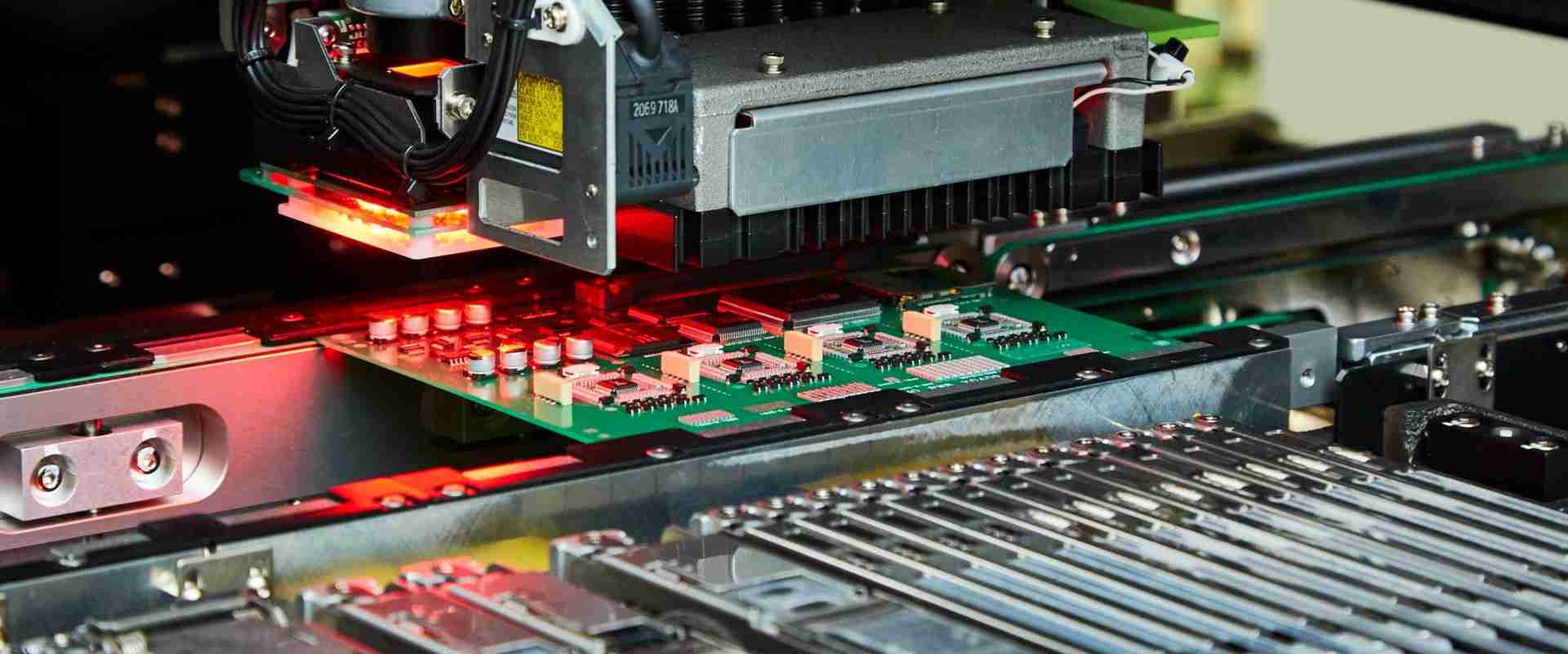
PCB Assembly Manufacturing is a complex process involving various steps, each critical to the functionality of electronic devices. This article provides a detailed overview of each step in the PCBA process, introducing the technologies and techniques employed at every stage.

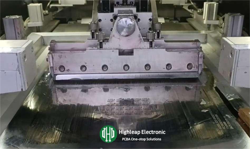
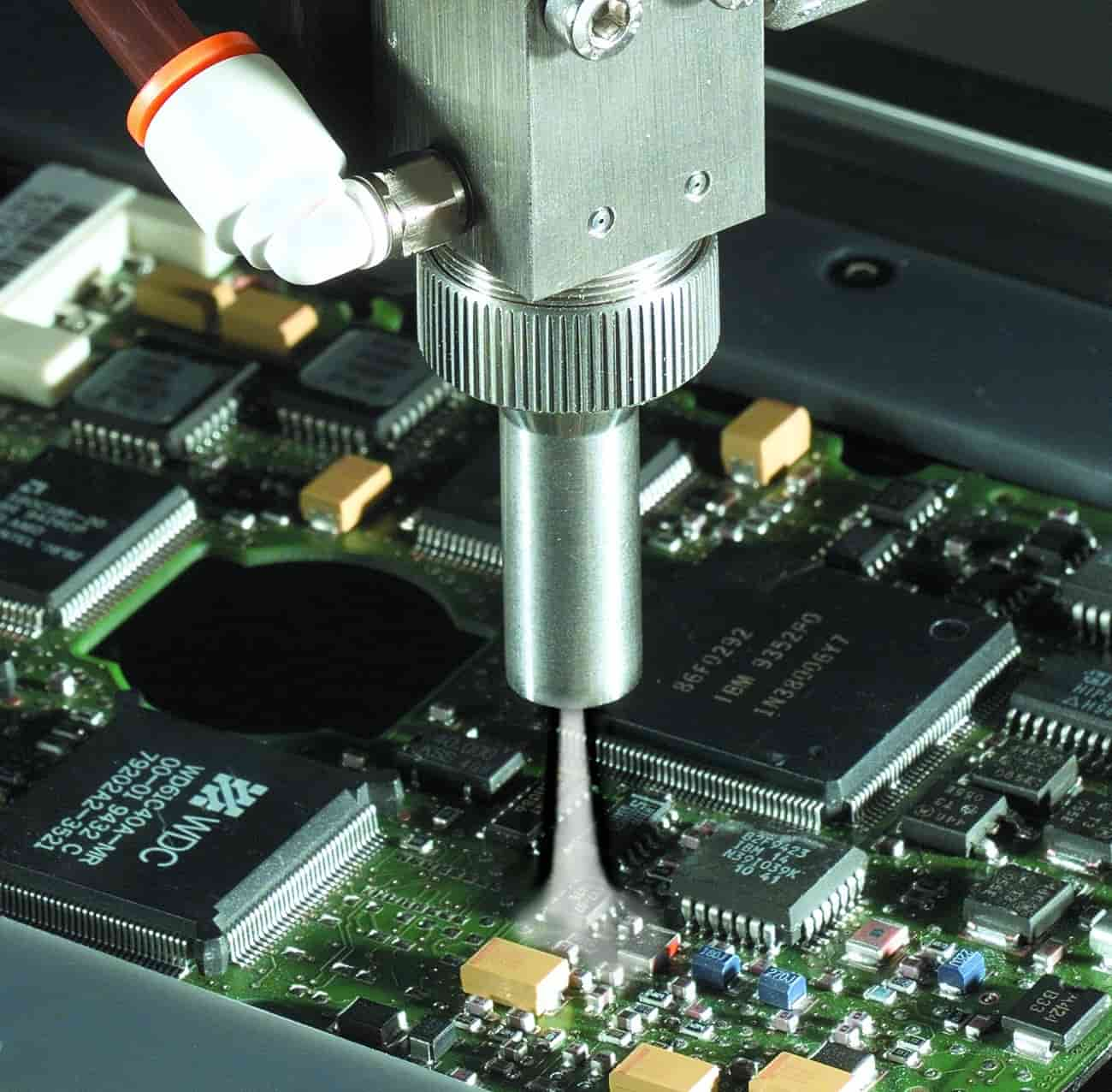
1. Solder Paste Stenciling

This is the first step where solder paste is applied to the board. A stencil is used to apply the paste only on the parts where components will be mounted.

=PCB Assembly Manufacturing Processes=

Electronic components are placed on the PCB. This step requires precision as components must align with the solder paste.

  • Automated Pick and Place Machines:These machines are the heart of the Pick and Place process. They use vacuum nozzles to pick up individual components from the feeders and precisely place them on their designated spots on the PCB.The latest machines are equipped with high-speed robotics, capable of placing thousands of components per hour with exceptional precision.

=PCB Assembly Manufacturing Processes==PCB Assembly Manufacturing Processes=3. Reflow Soldering

After placement, the board passes through a reflow oven where the solder paste melts and solidifies, forming a solid solder joint between the components and the board.

  • Conveyor Reflow Ovens: Provide controlled heating and cooling cycles.
  • Temperature Profiling: Ensures optimal heating for different types of components and solder.

=PCB Assembly Manufacturing Processes=4. PCB Assembly Manufacturing Inspection and Quality Control

Post-soldering, boards are inspected for defects like misalignment or insufficient solder.

  • Automatic Optical Inspection (AOI): Uses cameras to detect surface defects.
  • X-Ray Inspection: For checking solder joints under components.
  • 3D Solder Paste Inspection (SPI): Measures the solder paste volume and placement accuracy.

5. Through-Hole Component Insertion (if applicable)

For PCBs requiring through-hole components, these are inserted in this step.

  • Wave Soldering Machines: Used for soldering through-hole components.
  • Selective Soldering Machines: Provide precision soldering for specific areas on the PCB.

6. Final Inspection and Functional Testing

Ensures that the PCB functions as intended.

  • In-Circuit Testing (ICT): Checks the electrical functionality of the PCB.
  • Functional Testing Rigs: Simulate the operating environment of the PCB to ensure it functions correctly.

7. Conformal Coating (if required)

Applying a protective chemical coating to guard against environmental factors.

  • Spray or Dip Coating Techniques: Evenly apply the coating.
  • UV Curing Systems: Quickly cure the applied conformal coatings.

=PCB Assembly Manufacturing Processes=Application Methods:

Brushing: Manual application, suitable for low-volume or repair work.
Spraying: Can be manual or automated, providing a uniform coat over a larger area.
Dipping: Immersing the PCB in the coating material, ideal for high-volume production.
Selective Coating Machines: Precisely apply coating only on specified areas, avoiding connectors or heat sinks.

Types of Coating Materials:

Acrylics: Easy to apply and remove, offering basic protection against moisture and dust.
Silicones: Ideal for high-temperature environments, providing flexibility and protection against thermal shock.
Urethanes: Known for their robust chemical resistance, suitable for harsh chemical environments.
Epoxy: Offers excellent mechanical and chemical protection but can be challenging to remove or rework.
Parylene: Applied through a vapor deposition process, providing a very thin and uniform coating with excellent barrier properties.

8. Packaging and Shipping

The final step involves safely packaging the completed PCBAs for shipping.

Automated Packaging Lines: Ensure safe and efficient packaging.

The PCBA process is a blend of sophisticated technologies and meticulous techniques. Each step, from solder paste stenciling to packaging, plays a pivotal role in ensuring the reliability and functionality of the final electronic product. Advancements in automation, inspection technologies, and testing methods continue to enhance the efficiency and accuracy of the PCBA process. A thorough understanding of these processes is essential for anyone involved in electronic manufacturing, ensuring that PCBAs meet the highest standards of quality and performance.

PCB & PCBA quick quote

    Understanding Field-Effect Transistors (FETs) in PCB Design

    Understanding Field-Effect Transistors (FETs) in PCB Design

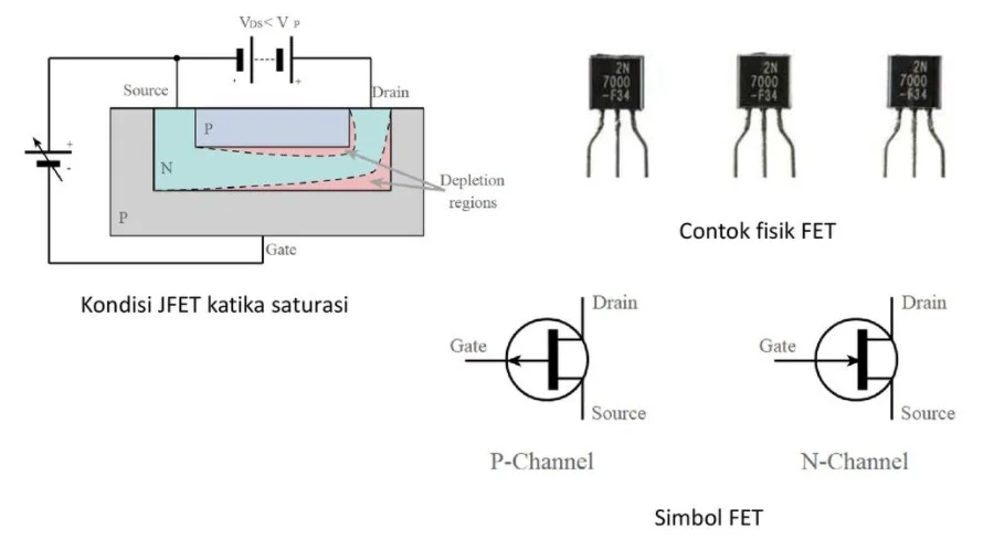
    Field Effect Transistors+FETIntroduction Field-Effect Transistors (FETs) are crucial components in modern electronics, serving as the backbone of various integrated circuits. Since Julius Edgar Lilienfeld first conceptualized the FET in 1926, these transistors have...

    Future Prospects and Challenges in Local Oscillator Development

    Future Prospects and Challenges in Local Oscillator Development

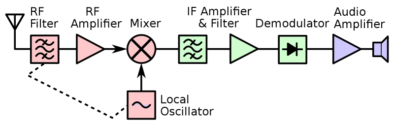
    Local Oscillator Block DiagramIn the realm of modern electronics, local oscillators (LOs) are indispensable components that significantly influence the functionality and efficiency of various devices. This article delves into the sophisticated world of local...

    Take a Quick Quote

    Discover how our expertise can help with PCBA project.