
Back to blog
How to Achieve Target PCB Impedance Control?

PCB Impedance Control
In the ever-evolving world of electronics, achieving precise control over PCB impedance has become a paramount concern for designers and engineers. As electronic devices continue to shrink in size and operate at astonishingly high frequencies, the ability to manage signal integrity has become more critical than ever. This comprehensive guide delves deep into the realm of PCB impedance control, shedding light on its significance, the influencing factors, and methods to attain target impedance with utmost precision.
Understanding PCB Impedance Control
PCB impedance control is the art of meticulously matching the characteristic impedance of traces on a printed circuit board to a predetermined design impedance. Achieving this harmony requires a meticulous approach to PCB trace dimensions, spacing, and routing. The primary goal is to create traces with a specific natural impedance that aligns with the design target, thereby preventing signal reflection and preserving signal integrity. The ramifications of disregarding impedance control can be severe, causing signal distortions such as overshoot, ringing, and crosstalk. These issues can wreak havoc, particularly when dealing with signals in the MHz and GHz range.
The Criticality of Impedance Control
Impedance control is a vital aspect of modern PCB designs, playing a crucial role in enhancing speed, reliability, and minimizing signal distortion. Particularly in high-frequency applications like RF communications, telecommunications, and high-speed analog video, maintaining precise impedance control for PCB traces is of utmost importance.
Impedance mismatches along PCB traces can lead to harmful signal reflections, causing disruptions to the integrity of the original signal. The severity of these distortions escalates with increasing impedance mismatches.
To address this issue, impedance control involves careful adjustment of trace dimensions and routing to ensure impedance matching across the entire PCB. This meticulous impedance matching significantly reduces reflections, safeguarding signals from corruption. For longer traces or higher frequency signals, tighter impedance control becomes even more critical in maintaining optimal signal clarity.
By implementing a thoughtfully designed layout, PCB designers can enhance impedance matching and preserve signal integrity. Meticulous impedance control allows PCBs to perform robustly even at GHz frequencies, meeting the demands of today’s high-speed electronics.
Factors Influencing PCB Impedance Control
Several key design elements influence the impedance of PCB traces and must be taken into account to achieve effective impedance control:
- Trace Width: The width of the copper trace plays a pivotal role in impedance control. Wider traces equate to lower impedance, while narrower traces increase impedance. To maintain impedance uniformity, traces must maintain consistent widths throughout their length. Any variation in trace width can disrupt impedance matching.
- Copper Thickness: The thickness of the copper trace impacts impedance due to its conductivity. Thicker copper translates to lower impedance, but extremely thick copper can complicate etching and plating processes. Most PCBs opt for 1-2 oz copper, striking a balance between controlled impedance and manufacturability.
- Dielectric Thickness: The thickness of the dielectric material between the trace and the reference plane is another influential factor. Thick dielectrics elevate impedance, but not linearly. Even a significant increase in dielectric thickness results in a modest impedance change. Thinner dielectrics require more precise control due to the larger impact of small variations.
- Dielectric Constant (Dk): The dielectric constant, or Dk, of the insulating base material has a profound impact on signal propagation. Materials with stable Dk values below 3 are ideal for controlled impedance at high frequencies. In contrast, materials like FR-4, with a higher Dk, can lead to inconsistent impedance control.
Achieving Target Impedance Control
Mastering PCB impedance control is an art that involves a combination of techniques and considerations:
Clearly Indicating Controlled Impedance Signals
When designing a PCB, it is crucial to clearly indicate which signals require controlled impedance. Component datasheets should specify the signal class and the corresponding impedance for each part. The preferred layer for routing each signal trace and spacing rules between traces carrying different signals should also be noted.
Choosing the Right Transmission Line
For high-frequency applications, selecting the appropriate transmission line structure is paramount. Microstrip lines, placed on the outer layer over a ground plane, are cost-effective and suitable for microwave circuits. Striplines, on the other hand, enclose the trace between ground planes within a multilayer PCB, offering tighter impedance control and reduced crosstalk at the expense of complexity.
Proper Spacing of Traces and Components
Adequate spacing between traces and components is vital to minimize crosstalk, especially in microstrip transmission lines carrying high-frequency signals. Adhering to spacing guidelines, such as 2-3 times the line width between traces, ensures impedance integrity and reduces coupling between traces.
Matching Trace Lengths
Matching the lengths of traces carrying related signals is crucial, especially for high-speed signals. Any discrepancy in trace length can lead to timing skew issues, causing problems with high-speed signals. Serpentine sections can be inserted in shorter traces to match overall lengths, ensuring synchronization.
Minimizing Capacitance Effects
It is advisable to avoid placing capacitive components between impedance-controlled traces, as capacitors can introduce impedance discontinuities that disrupt signal integrity. If capacitors must be used, they should be symmetrically placed across related traces to maintain consistent capacitive loading and equal signal propagation.
Conclusion
In the realm of high-speed PCB design, achieving and maintaining proper impedance control is an absolute imperative. By comprehending the factors that influence impedance and leveraging techniques such as balanced routing, length matching, and strategic component placement, PCB designers can unlock the potential of their designs. At Highleap, we pride ourselves on ensuring impedance control in every PCB we produce. With a wealth of experience across diverse applications, we stand ready to provide expert recommendations to help you achieve your controlled impedance goals. Contact us to explore our fabrication capabilities, focused on delivering unparalleled signal integrity and robust performance in high-speed circuits.
PCB & PCBA quick quote
Related Articles
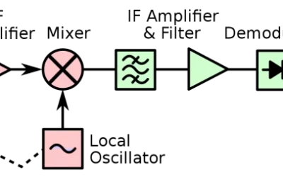
Future Prospects and Challenges in Local Oscillator Development
Developing multi-function chips that integrate local oscillators(LOs) with other RF components, such as mixers, amplifiers, and filters, is an emerging trend.

Understanding Silkscreen on PCB: A Comprehensive Guide for PCB Manufacturers
We will dive deep into the world of PCB silkscreen, exploring its significance, printing methods, design considerations, and much more.

What is the use of decoupling capacitors in PCB?
Decoupling capacitors, also known as bypass capacitors, are used to filter noise from power lines and stabilize voltage levels on ICs.