
Back to blog
Considerations for Signal Integrity in PCB Prototypes

Introduction
Signal integrity is a paramount concern in the realm of PCB prototypes. As electronic devices continue to evolve, the demand for higher data rates, enhanced functionality, and compact form factors places significant emphasis on maintaining signal integrity throughout the design and manufacturing process. This article delves into the profound significance of signal integrity in PCB prototypes, shedding light on the challenges encountered during the optimization process.
The Importance of Signal Integrity in PCB Prototypes
Signal integrity, in essence, signifies the capacity of a signal to traverse from the transmitter to the receiver without distortion or degradation. In the context of PCB prototypes, signal integrity is indispensable for ensuring the reliable and precise transmission of both digital and analog signals. By preserving signal integrity, users can effectively mitigate signal degradation, timing errors, electromagnetic interference (EMI), and crosstalk.
The optimization of signal integrity in PCB prototypes yields several critical benefits:
- Data Integrity: A robust signal path minimizes data errors, thereby ensuring dependable communication between components and subsystems.
- System Performance: Signal integrity optimization maximizes system performance by curbing signal degradation, ensuring timing precision, and minimizing signal reflections.
- EMI Compliance: PCB prototypes optimized for signal integrity can adhere to electromagnetic compatibility (EMC) regulations, thus reducing the risk of electromagnetic interference and circumventing costly redesigns.
Challenges in Optimizing Signal Integrity
While optimizing signal integrity is crucial, it is not without its challenges. Users often grapple with several intricacies, including:
- Component Placement and Routing: The precise placement of components and the routing of traces play pivotal roles in preserving signal integrity. Users must meticulously consider physical layouts, trace lengths, and impedance matching to minimize signal degradation and EMI.
- High-Speed Design: The proliferation of high-speed digital interfaces, such as DDR and PCIe, has added complexity to signal integrity considerations. Users must contend with impedance control, termination schemes, and skew management to avert signal degradation and timing errors.
- Power and Ground Plane Design: Adequate design of power and ground planes is imperative for sustaining signal integrity. Attention must be paid to plane splits, the placement of decoupling capacitors, and the minimization of loop areas to prevent noise coupling and ground bounce.
- Signal Integrity Analysis and Simulation: Precisely predicting signal integrity issues during the design phase remains a challenge. Signal integrity analysis and simulation tools serve as crucial aids in identifying potential problems such as reflections, crosstalk, and timing violations, empowering users to make informed design choices.
Addressing these challenges is pivotal for realizing robust PCB prototypes that align with the desired performance and functionality requisites.
Understanding Signal Integrity in PCB Prototypes
In the domain of PCB prototypes, comprehending signal integrity is foundational, as it profoundly influences the overall performance and reliability of electronic systems.

What is Signal Integrity?
Signal integrity entails the integrity and fidelity of electrical signals as they traverse through a PCB prototype. It encompasses a plethora of factors that influence signal behavior, including impedance matching, noise, reflections, crosstalk, and timing.
Signal integrity assumes a pivotal role in PCB prototypes since it directly influences data transmission accuracy, reliability, efficiency, and the overall system’s functionality. By ensuring optimal signal integrity, users can minimize errors, enhance data integrity, and reduce the risk of malfunctions in their PCB prototypes.
The Impact of Signal Integrity on Overall System Performance
Signal integrity exerts a profound impact on the overall performance of electronic systems, including PCB prototypes. Here are some critical facets of system performance influenced by signal integrity:
- Data Accuracy and Reliability: In PCB prototypes, signal integrity is the linchpin for data transmission accuracy and reliability. Distorted or degraded signals can culminate in data errors, leading to system malfunctions, diminished functionality, or complete system failure.
- Timing and Synchronization: Signal integrity issues like reflections, skew, and jitter can disrupt timing and synchronization within the system. Precise timing is paramount to ensuring proper data transfer and synchronization between components, especially in high-speed PCB prototypes.
- Signal Degradation and Loss: Signals can degrade or undergo attenuation in the absence of proper signal integrity. This leads to diminished signal quality and compromised system performance. Signal degradation can elevate bit error rates, minimize the signal-to-noise ratio, and reduce signal strength.
- Electromagnetic Interference (EMI): Poor signal integrity can engender electromagnetic interference, where signals interfere with each other, resulting in crosstalk and noise. EMI can disrupt signal transmission, introduce errors, and impact the performance of adjacent circuits and components.
Common Signal Integrity Issues and Consequences
Signal integrity issues manifest in various forms within PCB prototypes, each with its own set of consequences. Some commonplace signal integrity issues encompass:
- Reflections: Signal reflections materialize when signals encounter impedance mismatches or abrupt changes in transmission lines. Reflections can lead to signal distortion, timing errors, and signal integrity deterioration.
- Crosstalk: Crosstalk denotes the undesired coupling of signals between adjacent traces or components. It can culminate in signal interference, data corruption, and compromised signal integrity, especially in high-speed or densely populated PCB prototypes.
- Timing Violations: Timing violations arise when signals arrive at their destination incorrectly. These violations can trigger data errors, system instability, and reduced overall performance.
- Noise and Ground Bounce: Noise, spanning electromagnetic noise and power supply noise, can erode the quality of signals. Ground bounce, spurred by fluctuations in the ground reference voltage, can introduce noise and impact signal integrity.
A profound understanding of these common signal integrity issues is essential for users delving into PCB prototypes. By identifying and addressing these issues, users can optimize signal integrity, mitigate risks, and ensure the successful operation of their prototypes.
Key Considerations for Optimizing Signal Integrity in PCB Prototypes

Component Placement and Routing
Proper component placement and routing assume pivotal roles in the optimization of signal integrity in PCB prototypes. The ensuing considerations are paramount for achieving robust signal integrity:
- Impact of Component Placement: The arrangement of components on a PCB prototype profoundly influences signal integrity. Proximity of high-speed components reduces trace lengths, thereby minimizing signal degradation and timing errors. Careful placement also averts coupling between sensitive traces and reduces the risk of EMI.
- Routing Techniques: The employment of specific routing techniques is indispensable in curbing signal interference and crosstalk. Differential pair routing, for instance, ensures that paired signals remain in close proximity, thereby reducing mutual interference. Moreover, steering clear of sharp bends, crossing angles, and parallel traces mitigates signal reflections and EMI.
- Controlled Impedance Routing: Controlled impedance routing is imperative for sustaining consistent signal integrity in PCB prototypes. By guaranteeing that the impedance of transmission lines aligns with the source and load impedance, users can minimize signal reflections, bolster signal quality, and mitigate EMI. Meticulously calculated trace widths, spacing, and dielectric materials contribute to the realization of controlled impedance.
Power and Ground Planes
Power and ground planes hold sway in preserving signal integrity in PCB prototypes. The subsequent aspects warrant consideration for optimizing signal integrity:
- Role of Power and Ground Planes: Power and ground planes furnish low-impedance pathways for return currents, thereby diminishing the likelihood of noise coupling and augmenting signal quality. These planes double up as shielding mechanisms, curbing EMI and ensuring a stable reference voltage for signals.
- Proper Power and Ground Plane Design: To maximize signal integrity, users must ensure adept design and implementation of power and ground planes. Techniques like plane splits, stitching vias, and carving out dedicated zones for sensitive components can reduce noise and crosstalk. Sound layer stacking and balanced power distribution elevate signal quality and diminish EMI.
- Significance of Decoupling Capacitors: Decoupling capacitors occupy a critical position in suppressing power supply noise and sustaining stable voltage levels. Placing decoupling capacitors proximate to the power pins of components mitigates voltage fluctuations, reduces ground bounce, and ameliorates signal integrity issues. The judicious selection and placement of decoupling capacitors are imperative for effective noise suppression.
Signal Integrity Analysis and Simulation
Signal integrity analysis and simulation constitute invaluable tools for optimizing signal integrity in PCB prototypes. The following aspects merit attention:
- Signal Integrity Analysis Tools and Techniques: The employment of signal integrity analysis tools is indispensable for the early identification of potential issues during the design phase. Tools such as time-domain reflectometry (TDR), network analyzers, and electromagnetic simulation software empower users to scrutinize transmission line behavior, pinpoint signal degradation junctures, and validate design decisions.
- Benefits of Pre-layout and Post-layout Simulations: Pre-layout simulations enable users to dissect signal behavior and make informed design choices prior to PCB fabrication. Post-layout simulations validate the design’s integrity, accounting for component placement, routing, and layer stack-up. These simulations empower users to detect and rectify signal integrity issues, ensuring a resilient PCB prototype.
- Importance of Analysis Parameters: The analysis of reflections, signal integrity metrics (e.g., rise time, overshoot, undershoot), and eye diagrams assumes pivotal roles in evaluating signal quality and identifying potential issues. A profound grasp of these parameters empowers users to optimize trace geometries, termination schemes, and signal levels to meet the desired signal integrity objectives.
High-Speed Design Considerations
High-speed signals usher in unique challenges to signal integrity in PCB prototypes. The ensuing aspects warrant consideration when grappling with high-speed designs:
- Impact of High-Speed Signals: High-speed signals are particularly vulnerable to signal degradation, timing errors, and EMI. The accelerated edge rates and shortened signal lengths in high-speed designs demand specific considerations for signal integrity optimization in PCB prototypes.
- Controlled Impedance: The perpetuation of controlled impedance assumes heightened importance in high-speed designs. Accurate impedance matching minimizes signal reflections, guarantees signal integrity, and reduces the risk of signal degradation. The precision of trace width, spacing, and dielectric constant selection is pivotal for achieving controlled impedance.
- Termination and Skew Management: Proper termination techniques, encompassing series and parallel terminations, play a pivotal role in forestalling signal reflections and upholding signal integrity. Skew, denoting the variation in the arrival times of signals, can occasion timing errors and signal quality deterioration. Managing skew via length-matching techniques and controlled trace lengths is indispensable in high-speed PCB prototypes.
- Importance of Signal Integrity in High-Speed Interfaces: High-speed interfaces, such as DDR (Double Data Rate) and PCIe (Peripheral Component Interconnect Express), impose stringent signal integrity considerations. Failure to optimize signal integrity in these interfaces can precipitate data corruption, diminished performance, and system instability. A profound comprehension of the specific requirements and characteristics of these interfaces is imperative for successful signal integrity optimization.
By judiciously addressing these foundational considerations, users can markedly augment signal integrity in their PCB prototypes, ensuring reliable and high-performance operation. Optimized component placement and routing, adept power and ground plane design, utilization of signal integrity analysis and simulation tools, and adherence to high-speed design principles constitute crucial steps toward the realization of robust signal integrity.
PCB Prototype Testing and Validation
Testing and validation constitute cornerstone practices in optimizing signal integrity in PCB prototypes. This section delves into the significance of testing and validation, delineates various testing methodologies, and underscores the importance of iterative refinement based on testing outcomes.
The Significance of Testing and Validation
Testing and validation are indispensable facets of PCB prototyping, particularly in the context of signal integrity optimization. The primary objectives of testing and validation encompass:
- Verification of Signal Integrity: Testing empowers users to verify and authenticate the desired signal integrity parameters, such as rise time, overshoot, undershoot, and eye diagram characteristics. By comparing the measured results against the target specifications, users can assess signal quality and pinpoint areas necessitating enhancement.
- Identification of Design Issues: Testing aids in the discovery of potential design issues that impact signal integrity. By subjecting the PCB prototype to an array of tests, users can discern areas of concern, including impedance mismatches, reflections, crosstalk, and noise. Detecting these issues at an early juncture facilitates prompt design modifications and optimization.
- Assessment of Performance: Through testing and validation, users can gauge the performance of the PCB prototype under diverse operating conditions and scenarios. This assessment enables users to evaluate the prototype’s overall functionality, reliability, and robustness in real-world contexts.
Various Testing Methods
Several testing methodologies are commonly employed to evaluate signal integrity in PCB prototypes:
- Time-Domain Reflectometry (TDR): TDR measures impedance and identifies signal reflections along transmission lines. It aids in identifying impedance mismatches, signal degradation points, and discontinuities, thus enabling users to optimize trace geometries and impedance matching.
- Network Analyzers: Network analyzers enable comprehensive characterization and analysis of high-frequency electrical networks. They assess parameters such as impedance, S-parameters, and insertion loss, thereby assisting in the evaluation of signal integrity performance. Network analyzers furnish invaluable insights into the behavior of intricate circuits and components.
- Eye Diagram Analysis: Eye diagrams serve as visual representations of signal quality and integrity. They depict the opening and closure of the signal eye, offering insights into timing, noise, jitter, and signal distortion. Analyzing eye diagrams empowers users to assess signal quality and optimize the PCB prototype accordingly.
Prototype Iteration and Refinement
Testing and validation findings serve as compasses guiding the iterative refinement process of the prototype. Grounded in testing results, users can effect requisite design modifications and improvements to enhance signal integrity. Key considerations encompass:
- Trace Optimization: Adjusting trace widths, spacing, and routing configurations based on testing results helps minimize signal degradation, reflections, and crosstalk. Users can fine-tune the PCB layout to elevate signal integrity performance.
- Component Selection: Testing results may spotlight specific components that exert influence on signal integrity. Users can refine their component selection by weighing impedance requisites, signal quality, and noise susceptibility.
- Grounding and Decoupling: Testing may bring to the fore issues related to grounding and decoupling. Users can refine the grounding scheme, introduce additional decoupling capacitors, or optimize their placement to mitigate noise and amplify signal integrity.
Incorporating insights gleaned from testing and validation, users can iteratively hone the PCB prototype, optimize signal integrity, and realize the desired performance and reliability.
Conclusion
When it comes to signal integrity in PCB prototypes, several key considerations must be taken into account. These include ensuring proper component placement and routing, designing power and ground planes effectively, and utilizing signal integrity analysis and simulation tools. Additionally, high-speed design requires special attention, with a focus on controlled impedance, termination techniques, and skew management.
It is important to emphasize the importance of collaboration between users and PCB manufacturers to address signal integrity challenges effectively. By working together, they can optimize the design and manufacturing processes to achieve the desired signal integrity goals.
Furthermore, testing and validation play a critical role in the design process. Thorough testing and validation procedures help identify and rectify signal integrity issues, ensuring the reliability and performance of the PCB prototype.
By considering these factors and incorporating best practices, designers can enhance signal integrity in their PCB prototypes, leading to improved overall system performance and reliability.
PCB & PCBA quick quote
Related Articles
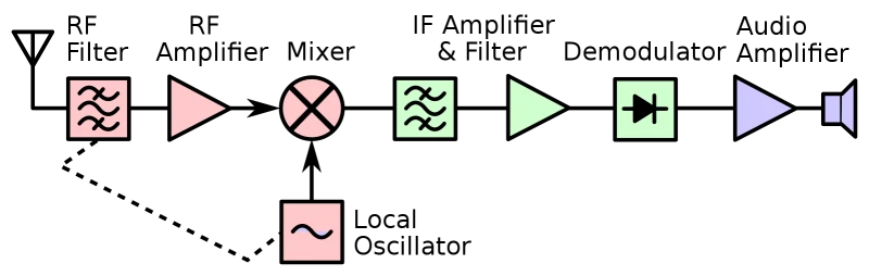
Future Prospects and Challenges in Local Oscillator Development
Local Oscillator Block DiagramIn the realm of modern electronics, local oscillators (LOs) are indispensable components that significantly influence the functionality and efficiency of various devices. This article delves into the sophisticated world of local...

Understanding Silkscreen on PCB: A Comprehensive Guide for PCB Manufacturers
PCB SilkscreenIntroduction PCBs form the essential infrastructure of modern electronics, providing a platform for the integration and interconnection of electronic components. While the functionality and electrical performance of a PCB are paramount, the aesthetic...

What is the use of decoupling capacitors in PCB?
decoupling capacitorIn the world of PCB design, decoupling capacitors play a vital role in ensuring the stability and performance of electronic circuits. These small but powerful components play an important role in reducing noise, maintaining voltage stability, and...
Take a Quick Quote