Back to blog
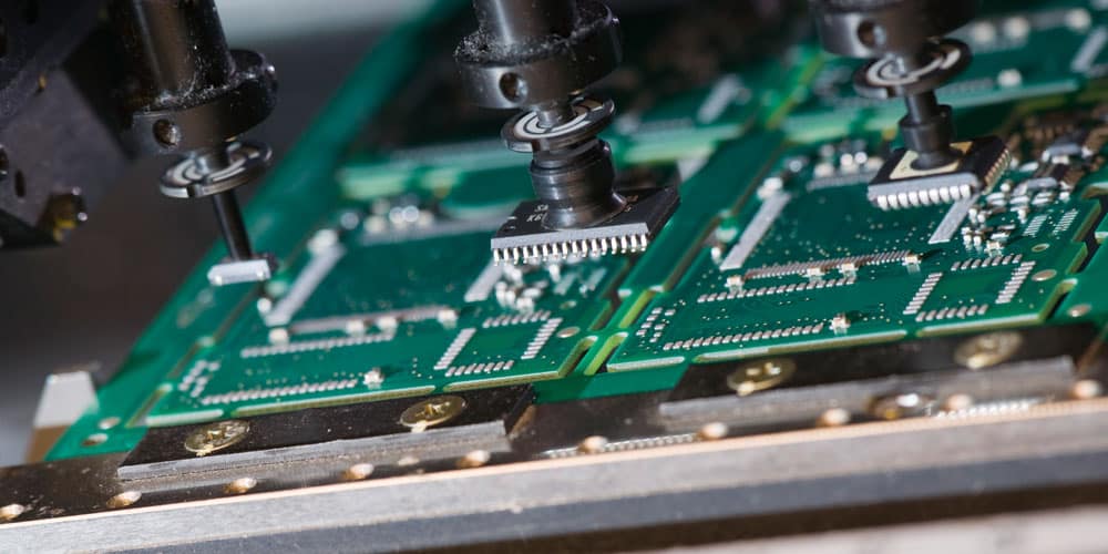
Complete PCB SMT Assembly Process Flow
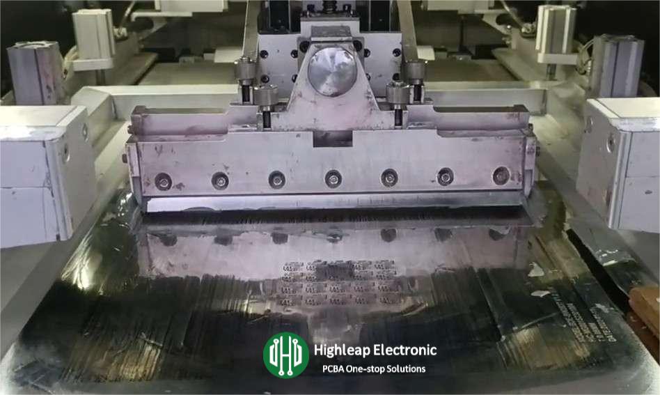
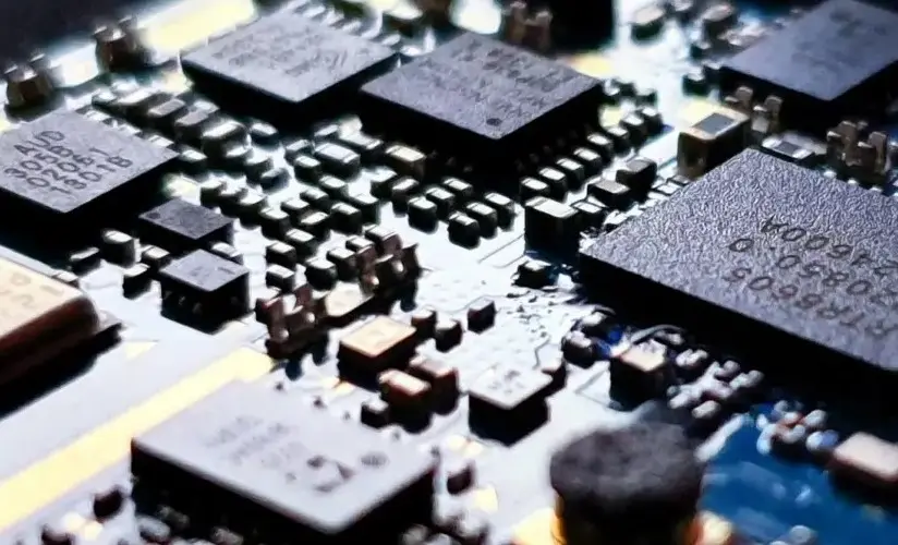
Print Solder Paste
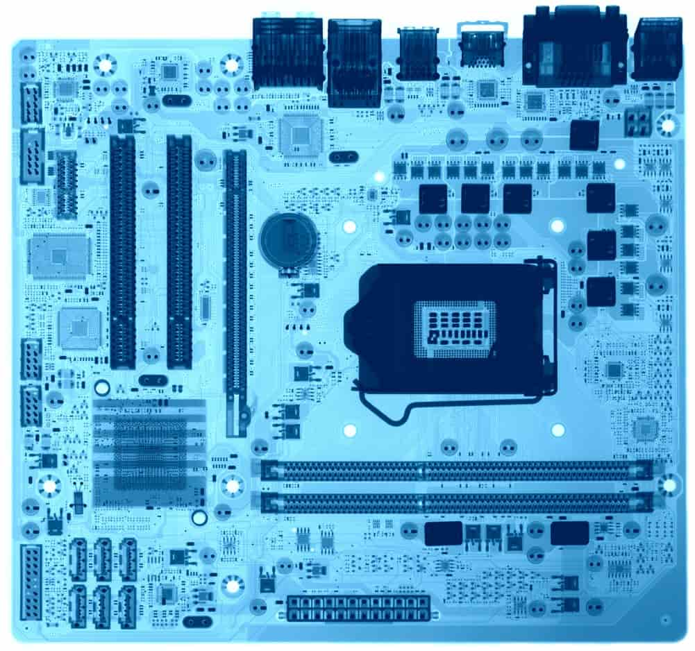
The first step in the PCB SMT assembly process is applying solder paste to the PCB. A stencil is used to precisely deposit the paste only on the pads where components will be placed. This paste acts as an adhesive and solder source for attaching components.
Print Solder Paste
Pick and Place SMT Component
Once the solder paste is applied, surface mount components are placed onto the board. This is done using automated pick-and-place machines, which accurately position each component on the designated solder paste pads.
SMT Assembly
Solder Paste Inspection (SPI)
After the solder paste application and before component placement, Solder Paste Inspection is conducted. This step ensures that the solder paste is applied correctly – checking for the right amount, shape, and placement. SPI helps prevent soldering defects that could occur during reflow.
Solder Paste Inspection
Reflow Soldering
In reflow soldering, the PCB with placed components is passed through a reflow oven. The oven heats the assembly to a point where the solder paste melts and forms solid solder joints, permanently attaching the components to the board.
Reflow soldering
Post-Reflow Inspection
After reflow soldering, the PCB is inspected to ensure all components are correctly soldered. Automated Optical Inspection (AOI) or X-ray inspection is often used for this purpose to detect any soldering defects like bridges, insufficient solder, or component misalignment.
AOI of PCB SMT assembly
AOI systems use high-resolution cameras to scan the PCBs for various types of defects such as soldering errors, missing or misplaced components, and other manufacturing faults.
Automated Optical Inspection (AOI)
X-ray inspection of PCB SMT assembly
X-ray inspection can see through the layers of a PCB, identifying hidden defects such as voids in solder joints, bridging, and solder quality issues within Ball Grid Arrays (BGAs), Micro BGA, and chip scale packages.
X-ray inspection
Final Inspection and Testing
This phase involves a thorough inspection and functional testing of the PCB. It ensures that the board meets all the required specifications and is functioning as intended. This step might include manual checks and various electrical tests.
Function Testing
Cleaning and Packaging
The final step is cleaning the PCB to remove any residual solder flux or contaminants. After cleaning, the PCB is carefully packaged for shipping or delivery to the next stage of production or assembly.
PCBA packaging
Each of these steps is critical in the PCB SMT assembly process, ensuring that the final PCB is of high quality and meets all necessary standards for performance and reliability. At Highleap Electronic, our one-stop solutions simplify your custom PCB & PCBA process. Tell us as specific as possible of your needs, provide the Gerber File or Bom List. We will work on the best solution according to your requirements, the specific quote will be provided within 24 hours
PCB & PCBA quick quote
Related Articles
How to Select the Best PCB Encapsulation Material for Your Project
PCB Encapsulation-PCB PottingIntroduction to Potting and Encapsulation Potting or encapsulation is a widely used method to protect circuit boards from damage, and it has proven to be effective. Different potting compounds are used in various circuit environments,...
What is the difference between SMD and SMT?
PCB SMTIntroduction to SMT and SMD Surface Mount Technology (SMT) and Surface Mount Devices (SMD) are crucial concepts in the field of electronics manufacturing, specifically in the assembly of printed circuit boards (PCBs). Both terms are integral to the modern...
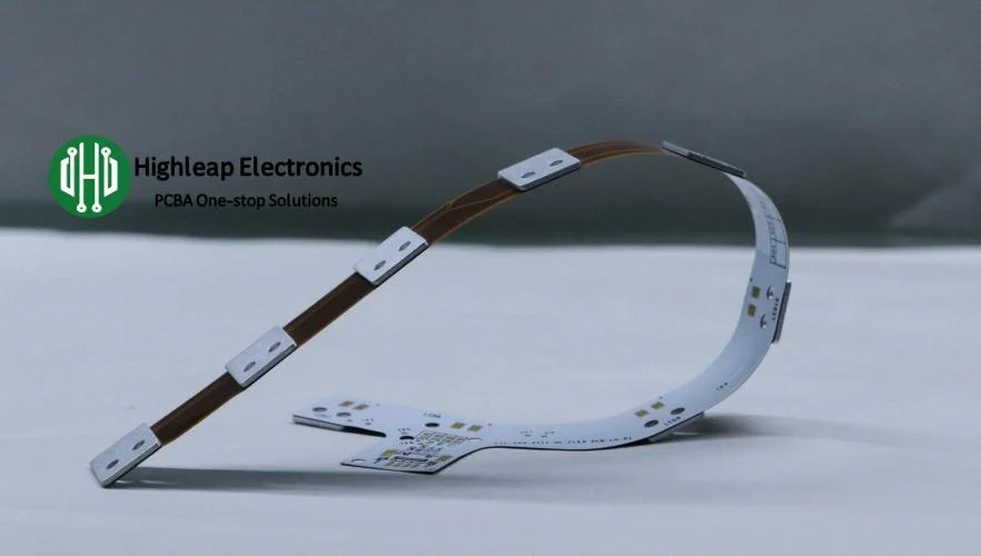
Flexible PCB Cost Optimization Strategy
flexible PCBIn the realm of contemporary electronics, the proliferation of flexible PCBs stands as a testament to the industry's evolution toward miniaturization and functionality. Unlike the more traditional rigid PCBs, which benefit from simpler production...
Take a Quick Quote