
Back to blog
Analysis of Power Supply Noise in HF PCB Design Process

Power Supply PCB Design Partial Files
In the realm of high-frequency PCB design, effective management of power supply noise is crucial to maintaining optimal system performance. As electronic devices evolve with higher clock speeds and increased component density, the impact of power supply noise becomes more pronounced. This comprehensive guide explores the complexities of power supply noise, its origins, and advanced techniques to mitigate its effects in high-frequency PCB designs.
Understanding Power Supply Noise
Power supply noise refers to unwanted electrical disturbances originating from the power distribution network within a PCB. These disturbances can manifest in various forms and significantly affect circuit performance, particularly in high-frequency applications where signal integrity is paramount.
Types of Power Supply Noise
1. Intrinsic Power Supply Noise:
-
- Switching Noise: Generated by DC-DC converters during switching operations.
- Ripple Voltage: Arises from inadequate filtering in power supply circuits.
- Thermal Noise: Resulting from resistive components within the power supply.
2. Extrinsic Power Supply Noise:
-
- Electromagnetic Interference (EMI): External noise introduced from nearby circuits or external sources.
- Ground Bounce: Caused by rapid changes in current, impacting ground potential.
- Crosstalk: Interference between adjacent power and signal lines.
3. Distributed Impedance Noise:
Non-ideal PCB power planes and traces contribute to distributed impedance, leading to:
-
- Voltage drops along power paths.
- Resonances within power planes.
- Localized voltage fluctuations near high-current components.
Analyzing Power Supply Noise in High-Frequency PCBs
To effectively mitigate power supply noise, understanding its behavior across different domains is crucial.
Frequency Domain Analysis
Power supply noise exhibits distinct spectral characteristics:
-
- Fundamental Noise Frequencies: Related to switching regulators.
- Harmonic Content: Multiple harmonics of fundamental frequencies.
- Broadband Noise: Extends into higher frequency ranges.
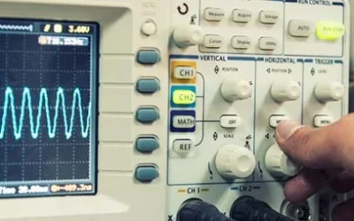
Time Domain Analysis
Oscilloscope measurements reveal temporal aspects of power supply noise:
-
- Voltage Ripple: Amplitude and frequency variations.
- Transient Response: Effects on circuit stability during load changes.
- Noise Correlation: Relationship with digital signal transitions.
Impedance Analysis
Using Vector Network Analyzers (VNAs) to analyze Power Distribution Network (PDN) impedance:
-
- Identifies resonances amplifying noise.
- Evaluates effectiveness of decoupling strategies.
- Sets impedance targets across frequency ranges.

CAM engineers optimize Gerber files
Best Practices for Power Supply Noise Mitigation
Implementing effective strategies is key to reducing power supply noise in high-frequency PCB designs:
Optimized PCB Stackup Design
-
- Dedicated Power and Ground Planes: Ensure low-impedance paths for power distribution.
- Split Planes: Isolate noisy and sensitive circuits effectively.
- Tight Coupling: Enhance performance by reducing plane inductance.
Advanced Decoupling Techniques
-
- Multi-Tiered Decoupling Strategy: Use capacitors of varying values for different frequency ranges.
- Low-ESR and Low-ESL Capacitors: Improve high-frequency decoupling efficiency.
- Embedded Capacitance: Utilize PCB stackup for ultra-high-frequency noise suppression.
Power Plane Design Optimization
-
- Stitching Vias: Connect power and ground planes to reduce inductance.
- Plane Cutouts: Isolate noisy areas from sensitive circuits.
- Guard Traces: Contain electromagnetic fields around high-speed signals.
Advanced Filtering Techniques
-
- Ferrite Beads: Suppress high-frequency noise effectively.
- LC Pi-Filters: Broadband noise reduction for critical circuits.
- Active Filtering: Minimize noise for ultra-sensitive applications.
Voltage Regulator Selection and Placement
-
- Low-Noise Linear Regulators: Suitable for noise-sensitive analog circuits.
- Point-of-Load (POL) Regulation: Ensure stable supply to sensitive components.
- Frequency Planning: Prevent interference in critical frequency bands.
Ground Design Strategies
-
- Single-Point Grounding: Suitable for low-frequency circuits.
- Multi-Point Grounding: Effective for high-frequency designs.
- Avoid Ground Loops: Optimize return path routing to prevent noise buildup.
EMI/EMC Considerations
-
- Shielding Techniques: Protect sensitive circuits from external EMI.
- Proper Cable Management: Minimize noise induction through careful routing.
- Ferrite Cores: Suppress common-mode noise in cables effectively.
Advanced Simulation and Analysis Tools
-
- 3D Electromagnetic Field Solvers: Accurately model PDN for noise analysis.
- SPICE Simulations: Analyze time-domain noise behavior.
- SI/PI Co-Simulation: Assess noise impact on signal integrity.
Power Supply Noise: Key Considerations for CAM Engineers
When creating engineering files related to “power noise,” CAM engineers should pay special attention to the following aspects:
- Power and ground plane design: Ensure optimized design of the power and ground planes in the Gerber file. This includes verifying good connectivity between the power and ground planes to minimize current loops and reduce parasitic inductance. Well-designed power and ground planes can effectively alleviate the propagation and interference of power noise. Carefully record the residual copper rate of each layer in the file. For layers that do not comply with specifications and fail to meet production requirements, promptly communicate and correct the files.
- Placement and optimization of vias: The placement of vias is crucial in Gerber files. For densely placed vias affecting production space distances, consider reducing or relocating them and communicate with the designer promptly. CAM engineers cannot modify the customer’s original design entirely. Verify whether the parameter information of each impedance pair aligns with the Gerber file, minimize impedance between different PCB layers, optimize the signal return path, and mitigate electromagnetic compatibility (EMC) issues. Correct via layout and connection are crucial for noise suppression in high-frequency PCBs, so boards with dense holes should be laid out logically.
- Optimization of trace width: Optimizing the trace width of power and ground lines in Gerber files has a significant impact on reducing power noise. Proper trace width design can lower resistance loss, decrease thermal noise generation, and improve power distribution efficiency. CAM engineers must ensure that the finalized engineering files meet production process requirements. Note relevant information in the ERP for special requirements. For complex figures, communicate with process engineers in advance to ensure compliance with high-frequency circuit specifications.
- Interlayer connection management: Effective management of interlayer connections in Gerber files directly influences the propagation and suppression of power noise. CAM engineers should ensure efficient use of interlayer connections (such as vias and jumpers) to minimize inductance and impedance in the power circuit, thereby reducing noise propagation paths. For impedance lines, mark attributes in advance for distinction. Adjustments are necessary for small board spacing and quantities to optimize production, with confirmation from the designer. For larger quantities, select other special processes to meet requirements. Avoid selecting complex processes without considering customer costs. CAM engineers should optimize Gerber files to facilitate factory production while saving costs for customers.
By focusing on these key considerations, CAM engineers can effectively manage power noise issues when generating Gerber files related to “power noise,” thereby enhancing PCB performance, signal integrity, and ensuring reliability and efficiency in the manufacturing process.
Conclusion
Effective management of power supply noise in high-frequency PCB design demands a holistic approach integrating theoretical insights with practical implementation strategies. By adopting advanced techniques and leveraging sophisticated tools, engineers can enhance the performance and reliability of high-frequency systems. As technology advances, staying informed about the latest developments in PCB design and component technologies remains essential for achieving superior noise management and ensuring long-term operational excellence.
FAQs
1. What role does component placement play in mitigating power supply noise in high-frequency PCB designs?
Effective component placement is crucial in minimizing power supply noise. By strategically positioning components, engineers can optimize signal paths, reduce parasitic effects, and minimize electromagnetic interference (EMI) propagation. This enhances overall circuit performance and ensures reliable operation in high-frequency applications.
2. How does thermal management affect power supply noise in high-frequency PCBs?
Thermal management plays a critical role in indirectly reducing power supply noise. By maintaining optimal operating temperatures, components perform more consistently, reducing thermal-induced noise sources such as resistive heating and thermal drift. Effective heat sinking and cooling strategies are essential to mitigate thermal noise and ensure stable circuit operation.
3. What considerations should be made regarding PCB material selection to minimize power supply noise?
PCB material selection significantly impacts power supply noise in high-frequency designs. Choosing materials with low dielectric loss and consistent electrical properties across frequencies helps to minimize signal attenuation and reflections. Additionally, materials with high thermal conductivity aid in efficient heat dissipation, indirectly reducing thermal-induced noise in the power distribution network.
4. How can electromagnetic compatibility (EMC) standards influence power supply noise management strategies?
Adherence to EMC standards is crucial for mitigating electromagnetic interference (EMI) and ensuring compliance with regulatory requirements. Implementing shielding techniques, proper cable management, and utilizing ferrite cores effectively suppresses common-mode noise and minimizes EMI-induced power supply noise. Engineers must integrate EMC considerations into their design process to achieve robust noise management and reliable circuit operation.
5. What advancements in PCB manufacturing technologies are enhancing power supply noise mitigation capabilities?
Recent advancements in PCB manufacturing technologies, such as embedded capacitance and advanced routing algorithms, are enhancing power supply noise mitigation capabilities. Embedded capacitance allows for ultra-high-frequency decoupling directly within the PCB stackup, reducing noise propagation paths and improving signal integrity. Moreover, advanced routing algorithms optimize signal paths and minimize impedance variations, further enhancing noise management in high-frequency PCB designs.

Related Articles
What is EMI, EMS and EMC?
At Highleap Electronic, we specialize in producing high-quality PCBs by integrating advanced techniques for impedance control, ensuring robust EMC and mitigating EMI.
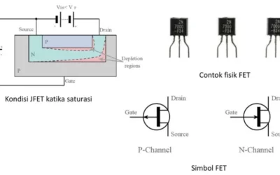
Understanding Field-Effect Transistors (FETs) in PCB Design
Dive into the fundamentals of Field-Effect Transistors (FETs) and their critical role in PCB design.
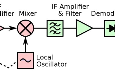
Future Prospects and Challenges in Local Oscillator Development
Developing multi-function chips that integrate local oscillators(LOs) with other RF components, such as mixers, amplifiers, and filters, is an emerging trend.
Take a Quick Quote