
Back to blog
How to Design a Power Supply PCB for Optimal Performance

Introduction
The design of a power supply PCB is a critical aspect of ensuring the reliable and efficient operation of electronic systems. Whether you’re working on a simple circuit or a complex application, a well-designed power supply PCB is essential. In this comprehensive guide, we will delve into the key considerations and steps involved in designing a power supply circuit board that meets the required specifications and ensures optimal performance. Let’s explore how to design a power supply PCB like a seasoned professional.
Understanding the Significance of Power Supply PCBs
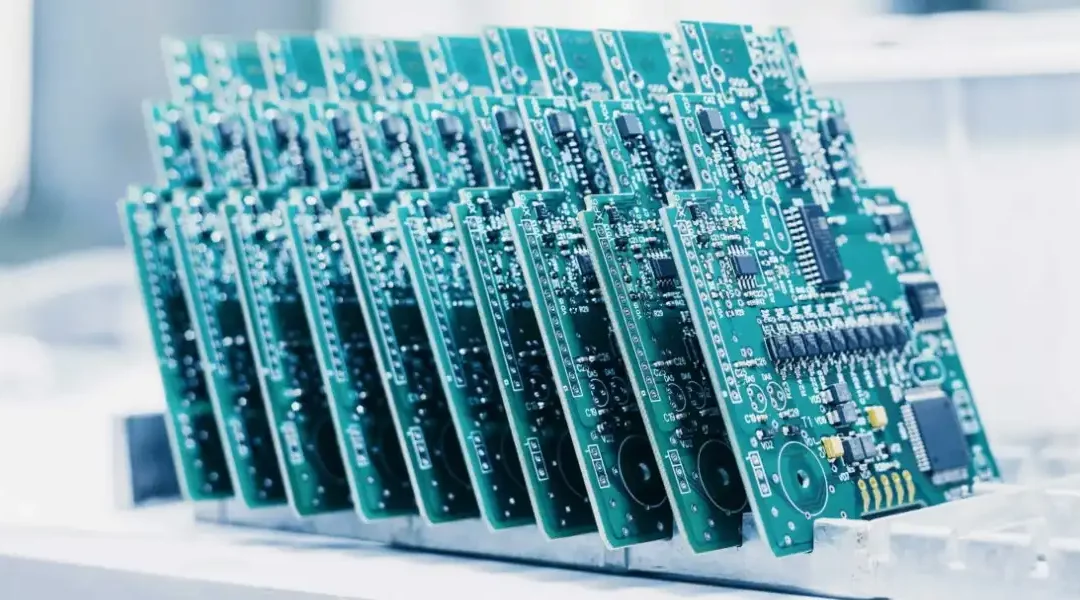
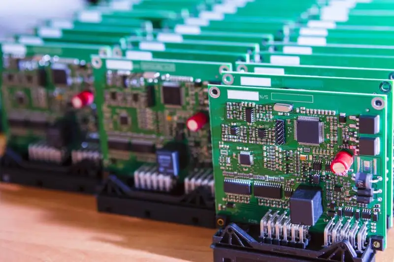
A power supply PCB serves as a specialized circuit board dedicated to regulating and distributing electrical power to various components or subsystems within electronic devices. Its primary function is to convert incoming electrical power from external sources, such as AC outlets or batteries, into the precise voltage and current levels required by the electronic device. Power supply PCBs are integral components of nearly all electronic devices, ranging from smartphones, laptops, and computers to household appliances, industrial machinery, and automotive systems. They ensure that the electronic components within these devices receive stable and reliable power, which is essential for their proper operation.
Key Considerations in Power Supply PCB Design
Choosing the Right Regulator
Selecting the appropriate regulator for your power supply PCB is a crucial decision. There are two main options: linear regulators and switched-mode regulators.
Linear Regulators: These regulators offer low noise output but have higher heat dissipation, often necessitating cooling systems. They require an input voltage higher than the desired output voltage due to a voltage dropout. While linear regulators are simple, cost-effective, and provide noiseless outputs, they suffer from significant power loss and lower efficiency. If you opt for a linear regulator, choose one with a low voltage dropout and perform thorough thermal analysis before fabrication.
Switched-Mode Regulators: In contrast, switched-mode regulators convert voltage by storing and releasing energy in inductors. They employ fast switching MOSFETs and offer highly efficient regulation. The output voltage can be adjusted by modifying the duty cycle of the Pulse Width Modulation (PWM). Switching regulators are more expensive and require additional passive components, but they have lower heat dissipation. Carefully assess your specific requirements before making a choice.
Selecting the Right Components
Choosing the appropriate components is vital for a successful power supply PCB design. Consider the voltage and current requirements of your application, and select components capable of handling the designated power levels. Pay attention to component types, packages, and footprints to ensure compatibility with your design and manufacturing constraints. Opt for reliable and reputable component suppliers to guarantee the quality and longevity of your power supply design.
Thermal Management
Efficient heat dissipation is critical to the performance of a power supply PCB. Electronic components generate heat as current flows through them, and maintaining lower temperatures is essential for better performance and component longevity. To address this, designers should incorporate proper cooling methods into their designs.
In the case of linear regulators, consider using heat sinks or other cooling mechanisms if the system allows for it. Fans can facilitate forced cooling, especially when dealing with high heat dissipation from specific devices.
Heat dissipation across the PCB may not be uniform, with certain components generating more heat and creating hotspots. To mitigate this, strategically place thermal vias near these components to efficiently transfer heat away from affected areas. By combining effective heat-dissipating techniques with appropriate cooling methods, designers can achieve highly efficient power supply designs that promote optimal performance and reliability.
Trace Routing
When it comes to trace routing, there are different approaches, such as routing during placement or after placement is complete. Regardless of the method you choose, ensure that your routing aligns with the component placement by using short and straight traces. Use traces with adequate width to handle current requirements and opt for 45-degree or rounded corners instead of right angles to minimize signal integrity issues.
Avoid using vias for power traces to prevent the introduction of inductance. Additionally, refrain from routing other signal traces under power components to prevent interference and maintain signal integrity.
Grounding Strategies
Achieving optimal grounding for the power supply is crucial. It is recommended to create a separate ground plane for power components. Utilizing a solid ground plane instead of routing with traces offers several advantages. Firstly, it provides an efficient grounding solution for the power supply. Secondly, it effectively isolates the noise generated by the current return paths onto a dedicated plane, keeping them separate from sensitive signal return paths on the common ground plane.
In the PCB layout, the two ground planes will ultimately establish a connection at a specific juncture, commonly designated as the ground via. This ground via is typically positioned within the thermal pad beneath the power supply IC. It serves the purpose of joining the two planes together while also providing a pathway for heat dissipation from the power supply. This connection holds particular significance in linear power supply designs.
Additionally, when designing linear power supplies, it is advisable to create a void in the ground plane specifically for high-gain devices. This minimizes potential noise interference and enhances the performance of these sensitive components.
Power Traces and Copper Pour
Calculating trace widths and ensuring proper copper thickness are essential for carrying the required current without excessive voltage drops or overheating. Utilize trace width calculators and PCB design software to determine appropriate trace widths based on current-carrying capacity. Additionally, consider implementing copper pour techniques to enhance heat dissipation and improve the overall thermal performance of your power supply PCB. Ground planes can be effectively utilized to minimize noise and improve signal integrity.
Power Integrity
Power integrity refers to the quality of power delivered to the circuit, measuring how effectively power is transferred from the source to the load within a system. It ensures that all circuits and devices receive the necessary power to achieve desired performance levels.
Maintaining power integrity involves minimizing noise in the power supply, as low noise levels contribute to higher power integrity. Designing for power integrity requires effective management of power supply noise. Various simulation tools are available for estimating power quality within a circuit. These tools predict voltage drops, recommend the placement of decoupling capacitors, and identify areas of high current flow, known as hotspots, within circuits.
Conclusion
Designing a power supply PCB requires meticulous attention to numerous factors. By adhering to this comprehensive guide, you can create power supply PCBs that meet the necessary specifications and deliver dependable and efficient performance.
As a renowned PCB manufacturer, Highleap Electronic offers an extensive range of state-of-the-art equipment and expertise in processing power supply PCBs. We are capable of customizing power supply PCB solutions according to your specific needs, from design to manufacturing and testing. For a free consultation, click here.
In conclusion, mastering the art of power supply PCB design is essential for engineers and designers working on electronic systems. With the right knowledge and attention to detail, you can create power supply PCBs that ensure the reliable and efficient operation of a wide range of electronic devices. Whether it’s a linear regulator for an industrial application or a switched-mode regulator for a portable device, the principles of power supply PCB design remain critical for achieving optimal performance and functionality.
PCB & PCBA quick quote
Related Articles

Automotive PCBs: Design,Manufacturing and Applications
Automotive PCBThe integration of advanced electronic systems in vehicles has revolutionized the automotive industry, significantly enhancing both safety and performance. At the heart of this technological evolution are PCBs, which are essential for the functionality...
How to Choose the Right Smart Home PCB – PCB Manufacturing
Smart Home PCBAThe concept of a "smart home" has evolved significantly in the digital age, primarily due to advancements in Internet of Things (IoT) technology and smart devices. The Smart Home PCB represents a vital element in the design, manufacturing, and...
Tailored PCB Manufacturing Services for Consumer Electronics
Consumer Electronics PCBAAt Highleap Electronic, we specialize in delivering high-quality optimized interconnect solutions tailored specifically for the dynamic world of consumer electronics. Our extensive range includes single-, double-, or multi-layered printed...
Take a Quick Quote