
Back to blog
The Best PCB Design Guidelines for Reduced EMI
In the world of electronics, designing PCBs that effectively mitigate Electromagnetic Interference (EMI) is a paramount concern. EMI, often seen as an unwanted side effect of electronic circuits, can hinder the normal operation of electronic devices and lead to potential performance issues. In this comprehensive guide, we will delve into the sources of EMI, distinguish between Electromagnetic Compatibility (EMC) and EMI, and present detailed and professional PCB design guidelines for significantly reducing EMI in your designs.

Understanding Electromagnetic Interference
To gain a comprehensive grasp of dealing with EMI in PCB design, it is imperative to commence with a thorough comprehension of the underlying physics governing this phenomenon. EMI, which stands for Electromagnetic Interference, is rooted in the fundamental forces of nature, particularly electromagnetism. Electromagnetism exhibits itself through both electric and magnetic forces, which play pivotal roles in the functionality of electronic devices.
The genesis of EMI can be traced back to the flow of electric current within a closed circuit. As electric current courses through this circuit, it generates a magnetic field that extends outward, oriented perpendicular to the direction of current flow. This emitted energy forms electromagnetic waves and has the potential to disrupt neighboring electronic components and signal pathways. Consequently, this interference results in EMI-related issues that necessitate efficient management strategies. An in-depth understanding of these principles serves as a solid foundation for addressing EMI challenges effectively in PCB design.
EMC vs. EMI: Clarifying the Distinction
Electromagnetic Compatibility (EMC)
EMC is a comprehensive concept in the field of electrical and electronic engineering. It focuses on the ability of various electronic devices, components, and systems to operate in close proximity to each other without causing or suffering from electromagnetic interference. The core objective of EMC is to ensure the harmonious coexistence of these elements within a shared electromagnetic environment. Here are some key aspects of EMC:
- Harmonious Coexistence: EMC seeks to establish a scenario where electronic devices can function together without causing disruptions or failures due to electromagnetic interference. This involves both emission control (reducing unwanted emissions) and immunity (resistance to external interference).
- Emission Control: EMC involves managing the electromagnetic emissions generated by electronic devices. This includes controlling the radiated and conducted emissions to prevent them from interfering with other nearby devices.
- Immunity: Immunity in EMC refers to a device’s ability to withstand electromagnetic interference from external sources without malfunctioning. Electronic systems should be designed to be robust against common sources of interference, such as electromagnetic fields from power lines or other electronic devices.
- Compliance Standards: Various regulatory bodies and standards organizations, such as the Federal Communications Commission (FCC) in the United States and the International Electrotechnical Commission (IEC), have established EMC standards. Compliance with these standards is essential for electronic products to be legally sold and used in many regions.
- Design Considerations: Achieving EMC involves careful design practices, including proper grounding, shielding, and filtering. Designers must also consider factors like signal integrity, crosstalk, and power distribution to minimize electromagnetic interference.
- Testing and Certification: EMC testing is a crucial step in ensuring that electronic products meet the required EMC standards. Products must undergo testing to confirm that they do not emit excessive electromagnetic radiation and can withstand external interference.
Electromagnetic Interference (EMI)
EMI is a subset of EMC and refers to the unwanted electromagnetic emissions or disturbances caused by electronic devices, components, or systems. EMI occurs when electromagnetic radiation or conducted electrical noise from one device interferes with the operation of another nearby device. Here are key aspects of EMI:
- Sources: EMI can originate from a variety of sources, including digital logic circuits, switching power supplies, high-frequency components, and other electronic elements that generate electromagnetic fields.
- Types of EMI: EMI can manifest in different forms, such as radiated EMI (emissions transmitted through the air) and conducted EMI (emissions conducted through wires or traces on PCBs).
- Effects: EMI can have detrimental effects on electronic devices and systems. It can lead to data corruption, communication errors, equipment malfunction, and even safety hazards in critical applications.
- Mitigation: To reduce EMI, engineers employ techniques like electromagnetic shielding, filtering, grounding, and careful PCB layout. These measures help contain and minimize unwanted emissions, ensuring that devices comply with EMC standards.
- Frequency Spectrum: EMI can occur across a wide range of frequencies, from low-frequency power line disturbances to high-frequency radio frequency interference. Understanding the frequency spectrum of EMI is essential for effective mitigation.
In summary, EMC is the overarching concept focused on ensuring the harmonious coexistence of electronic devices within a shared electromagnetic environment, while EMI specifically deals with the unwanted interference caused by these devices. Engineers and designers must address both EMC and EMI considerations to create reliable and interference-free electronic systems.
Sources of PCB EMI
To effectively address EMI in PCB design, it is vital to identify the various sources from which it can originate. EMI can arise both from within the PCB and from external sources, and understanding these sources is the first step in mitigating their impact.
1. EMI from Components
High-power electronic components, such as processors, FPGAs, amplifiers, transmitters, and antennas, can significantly contribute to EMI. Additionally, switching components, which rapidly change their state, can generate disruptive interference. To reduce EMI from components:
Select Low-Power Consumption Parts:
One of the primary generators of EMI on circuit boards are components that require significant power. Whenever possible, opt for low-power alternatives that do not compromise functionality or quality.
Component Isolation:
A best practice in design is to place components that process similar types of signals in close proximity and separate them from components handling different signal types. For example, digital components should be grouped with other digital parts and isolated from analog devices.
Utilize PCB Fencing:
Enclose sensitive components or sub-circuits within shielding structures such as PCB guard rings and Faraday cages. These structures are highly effective in reducing radiation into the surrounding environment.
Implement Heat Dissipation Techniques:
Electronic components generate heat as a byproduct of their operation. Efficient heat sinks and well-placed vias can aid in heat dissipation, contributing to EMI minimization.
2. EMI from Signals and Traces
EMI can also be created along signal traces and at pin and connector points on the PCB. Several factors contribute to EMI in this context, including unbalanced differential pair routing, stray capacitance, and signal reflections.
Employ Adequate Clearance Between Signal Traces:
One of the most critical factors in reducing EMI between traces is ensuring adequate spacing or clearance. Adhere to the recommendations provided by your CM (Contract Manufacturer), often based on IPC standards, to determine the appropriate clearance.
Ground Decoupling and Bypass Capacitors:
Stray capacitance is challenging to avoid, but its effects can be mitigated by grounding capacitors as close to the pins as possible.
Utilize Effective EMI Filtering:
Many designs, especially those involving digital signals, feature switching devices that can create signal distortion. The most effective way to improve signal fidelity in such cases is by implementing proper EMI filtering.
Minimize the Length of Return Paths:
Ground return paths should be as short as possible to reduce loop areas, which can be sources of EMI.
Ensure Identical Characteristics for Differential Traces:
In the case of differential signal paths, it is essential that trace pairs are mirrored accurately. This includes maintaining consistent trace lengths, copper weights, and a constant separation. When necessary, meandering can be employed to achieve and preserve these characteristics.
Avoid Sharp Angles:
When routing traces, opt for rounded edges rather than sharp corners. Sharp corners can lead to signal reflections due to modifications in characteristic impedance.
Avoid Placing Conducting Layers Next to Each Other:
Never position two conducting layers directly adjacent to each other in the PCB stackup. Adequate separation, typically by a ground plane, is crucial.
3. EMI from External Sources
In addition to internal sources, external factors can introduce EMI to the PCB. This external interference can affect not only the circuit’s operation but also the electromagnetic compatibility of the entire system.
Use Shielding:
Shielding is typically applied to specific components or sub-circuits. Unlike fencing, shielding structures are often constructed from insulating materials and placed over the top of components or enclosures, effectively isolating them from external EMI sources.
Consider Enclosures:
While enclosures are primarily viewed as safety devices, they can also serve as effective protection against debris and external EMI sources. Enclosed PCBs are shielded from external influences, ensuring their reliable operation.
Optimizing PCB Design for EMI Reduction
While the above guidelines provide a solid foundation for EMI reduction in PCB design, it’s important to note that specific requirements may vary based on the design’s complexity, functionality, and performance objectives. To achieve optimal EMI reduction, engineers should strive to optimize their designs by employing advanced analysis tools.
Tailoring EMI Reduction Strategies to Specific Designs
1. Complexity Matters
The complexity of a PCB design plays a pivotal role in determining the extent of potential EMI issues. More intricate designs often involve a higher density of components, densely packed traces, and intricate signal paths. As a result, the likelihood of EMI interference increases proportionally.
Component Placement:
In complex PCBs, meticulous attention must be given to the placement of components. Grouping similar components together while ensuring they are isolated from dissimilar ones remains crucial. Advanced EDA (Electronic Design Automation) tools provide automated component placement features that help optimize component arrangements for EMI reduction.
Layer Stackup:
Complex designs may necessitate multilayer PCBs. Properly configuring the layer stackup is essential to minimize EMI. Careful consideration of the order and distance between conducting and ground planes is vital. Simulation tools can assist in determining the optimal stackup configuration.
2. Functionality and Performance Objectives
The intended functionality and performance objectives of a PCB can significantly impact EMI reduction strategies. PCBs designed for high-speed data transmission, such as those used in telecommunications or data centers, often require stricter EMI mitigation measures due to the sensitivity of the signals involved.
Differential Signaling:
For high-speed designs, the use of differential signaling is common to reduce susceptibility to common-mode EMI. Differential pairs should be carefully designed with controlled impedance and consistent trace lengths. Advanced PCB design tools enable precise impedance matching for differential pairs.
Filtering and Decoupling:
High-performance PCBs benefit from advanced filtering and decoupling techniques. Engineers should select high-quality components like EMI filters and capacitors with appropriate capacitance values to suppress noise effectively. Simulation tools can aid in evaluating the effectiveness of these components.
Advanced Analysis Tools for EMI Reduction
Achieving optimal EMI reduction often necessitates the use of advanced analysis tools and simulation software. These tools empower engineers to thoroughly evaluate and refine their designs, ensuring they meet stringent EMI requirements.
1. Electromagnetic Co-Simulation
Electromagnetic co-simulation capabilities enable engineers to assess the electromagnetic behavior of PCB layouts. This feature allows for the identification and mitigation of potential EMI issues at an early design stage.
3D Visualization:
3D visualization tools provide insights into component placement, signal routing, and potential EMI sources. Engineers can use this feature to optimize component placement for EMI reduction.
2. PSpice Advanced Analysis
PSpice Advanced Analysis is a powerful simulation tool that can be instrumental in EMI reduction:
Signal Integrity Analysis:
Engineers can leverage PSpice to conduct thorough signal integrity analysis. By simulating signal behavior under various conditions, including EMI-induced noise, they can identify potential vulnerabilities and implement mitigation strategies.
Heat Dissipation Analysis:
Efficient heat dissipation is integral to EMI reduction. PSpice enables engineers to analyze heat distribution within the PCB, aiding in the design of effective heat dissipation solutions.
Source-Targeted Analysis:
PSpice’s source-targeted analysis capabilities allow engineers to pinpoint EMI sources and their effects on specific signal paths. This granular approach facilitates precise EMI reduction measures.
3. Electromagnetic Simulation Software
Dedicated electromagnetic simulation software provides in-depth analysis of electromagnetic behavior. These tools are particularly valuable for high-frequency and RF (Radio Frequency) designs where EMI reduction is critical.
Conclusion
In conclusion, mastering the art of PCB design for EMI reduction is paramount in ensuring the flawless operation of electronic devices and achieving Electromagnetic Compatibility (EMC) in a wide range of applications. By comprehending the sources of EMI and diligently adhering to the recommended guidelines, engineers can craft printed circuit board assemblies (PCBAs) that meet stringent EMC standards and perform reliably.
Furthermore, it’s important to recognize that EMI mitigation is not a one-size-fits-all approach. Complex designs with varying functionality and performance objectives may require tailored strategies and advanced analysis tools. Leveraging electromagnetic co-simulation, advanced analysis tools like PSpice, and dedicated electromagnetic simulation software empowers engineers to identify and address potential EMI issues at an early stage, resulting in more robust and EMC-compliant PCB designs.
In today’s fast-paced electronics industry, where devices continue to become smaller, faster, and more interconnected, the ability to effectively manage EMI is a critical skill that separates successful designs from those plagued by interference-related issues. By staying updated on the latest EMI reduction techniques and utilizing cutting-edge design tools, engineers can create electronic systems that not only meet regulatory requirements but also excel in performance and reliability.
PCB & PCBA quick quote
Related Articles
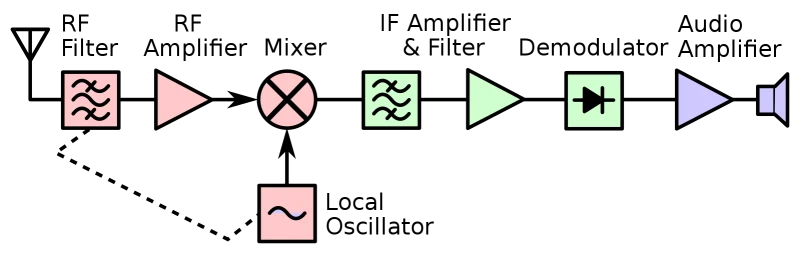
Future Prospects and Challenges in Local Oscillator Development
Local Oscillator Block DiagramIn the realm of modern electronics, local oscillators (LOs) are indispensable components that significantly influence the functionality and efficiency of various devices. This article delves into the sophisticated world of local...

Understanding Silkscreen on PCB: A Comprehensive Guide for PCB Manufacturers
PCB SilkscreenIntroduction PCBs form the essential infrastructure of modern electronics, providing a platform for the integration and interconnection of electronic components. While the functionality and electrical performance of a PCB are paramount, the aesthetic...

What is the use of decoupling capacitors in PCB?
decoupling capacitorIn the world of PCB design, decoupling capacitors play a vital role in ensuring the stability and performance of electronic circuits. These small but powerful components play an important role in reducing noise, maintaining voltage stability, and...
Take a Quick Quote