
Comprehensive Guide to RF PCB Design
RF PCB Design Considerations
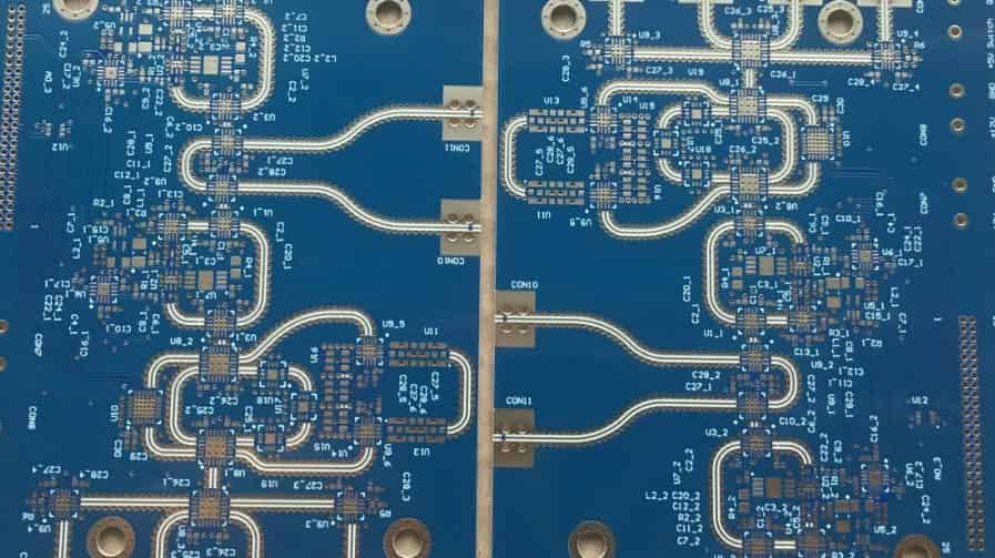
Radio frequency (RF) PCBs carry high-speed signals for wireless communications, radars, satellite networks and other electronic applications. RF circuits demand tightly controlled impedance, effective shielding, and layout optimization for signal integrity. Here are key guidelines for successful RF PCB design.
Understand Requirements
- Operating frequency range
- Input/output power levels
- Signal types – analog, digital, mixed
- Number of layers needed
- Impedance control requirements
- Primary routing paths
- Shielding needs
- Thermal design constraints
- Technology nodes for active components
- Applicable standards compliance
Choose Proper Materials
- Substrate dielectric constant suited for frequency (ceramics, PTFE, low-loss laminates)
- Dielectric materials with tight tolerances
- Copper thickness and plating – 1 oz, 2 oz or thicker
- High performance conductor finishes
- Proper foil type – standard, modified, hyperbolic
- Adequate layer count for routing density
- Thick cores for heat sinking
Control Impedance
- Determine target impedance based on sources, loads (typically 50Ω or 75Ω)
- Use plane layers for impedance control rather than traces
- Select dielectric thickness, copper weight, widths to achieve target impedance
- Define impedance requirements in fab notes
- Use impedance calculators to estimate dimensions
- Perform 3D field solving for high accuracy models
- Specify tight impedance tolerances to fab house
Isolate Noisy Circuits
- Keep noisy digital routing on inner layers, use ground planes around
- Use shielded clock and data lines if possible
- Enclose switching-mode supplies in metal channels
- Shield or filter any interfaces that could couple noise
Manage Layers
- Ground and power plane layers for low impedance current flow
- Signal layers spaced out with ground planes between for isolation
- Flood unused areas on inner layers with copper
- Dedicate bottom layer for components, top layer for RF traces
Optimize Component Placement
- Position active components first considering isolation needs
- Place bypass/decoupling capacitors close to ICs
- Orient components to optimize interconnect routing
Route Efficiently
- Use 45°angled traces rather than 90°bends
- Route critical nets before less critical ones
- Create routing channels to group related signals
- Plan main runs first, then drop-downs to devices
- Use curved/tapered bends for impedance continuity
- Avoid acute angles that cause reflections
By following these guidelines during layout, RF PCBs can achieve target performance in wireless, radar and communication systems with tightly integrated electronics.
Factors Impacting RF PCB Design
Designing printed circuit boards for radio frequency (RF) applications requires managing various parameters to ensure signal integrity and performance. Here are key factors that influence high-frequency PCB design.
Operating Frequency
- Higher frequencies demand tighter layout geometries
- Trace widths must shrink to control characteristic impedance
- Rise times shorten requiring matched trace lengths
- Losses increase necessitating low-loss dielectrics
- Component parasitics significantly impact performance
Dielectric Material
- Permittivity affects propagating impedance
- Low-loss tangents minimize signal attenuation
- Tight tolerances aid impedance control
- Moisture absorption degrades performance
- Thermal properties influence heating
Copper Thickness
- Thicker copper lowers losses
- Outer layer thickness impacts impedance
- Plating uniformity essential for consistency
- Weights from 1 to 6+ oz used in RF designs
Layer Stackup
- Thin dielectrics needed for fine lines/spaces
- More layers allow isolation and shielding
- Layer sequence impacts performance, cost
- High layer counts improve routing density
Controlled Impedance
- Matched impedance prevents reflections
- Calculated based on dielectric, dimensions, copper
- Tight impedance control mandatory
- Field solving refines calculated values
Passive Integration
- Embedded passives save space over discrete
- Right values must be chosen for function
- Reduces parasitics of external components
- Passive layers take away routing layers
Shielding
- Prevents coupling between circuits
- Full enclosure or selective shielding used
- Ground planes isolate layer routing
- Plated through-holes connect shields
Thermal Management
- RF ICs produce significant heat needing removal
- Thermal cores and copper layers spread heat
- Thermal vias help conduct heat away
- Fans and heatsinks used for force convection
By understanding and optimizing these parameters, RF PCBs can deliver precision performance in high-speed wireless, radar, communication and other leading-edge electronic systems.
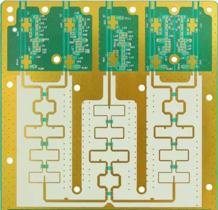
High Frequency PCB Characteristics
Printed circuit boards supporting radio frequency (RF) applications beyond 1 GHz demand special design considerations for signal integrity. Here are key characteristics of high frequency PCBs:
Controlled Impedance
- Matched impedance required for clean signal propagation
- Achieved through dielectric constant, copper weight, trace dimensions
- Field solvers used to accurately model routing impedance
Low Loss Materials
- Specialized low-loss laminates with tight tolerances
- PTFE, ceramic filled and hydrocarbon thermosets commonly used
- Lower loss tangents reduce high frequency attenuation
High Layer Count
- Additional layers allow proper isolation and shielding
- Layer counts from 6 to 20+ needed for complex designs
- More layers provide routing flexibility
Fine Geometry
- Narrow trace widths and tight spaces control impedance
- Small features needed for high density layouts
- Tight registration accuracy essential
Controlled Environment
- Materials with low moisture absorption preferred
- Delamination risks increase with more layers
- Careful handling and storage required
Advanced Modeling
- 3D electromagnetic field solvers used for analysis
- Critical to predict resonances, coupling and radiation
- Verifies controlled impedance prior to fabrication
Tight Tolerances
- Fabrication process control crucial for RF performance
- Impedance, dielectric constant, conductor profiles
- Statistical process control improves consistency
Testability
- Test points, ports and fixtures required for validation
- Equipment for measuring frequency, power, modulation
- Debugging ability needed for field failures
Adhering to these design principles enables RF PCBs to perform in demanding wireless, radar, communications and other high-frequency applications.
PCB Stackup Configuration
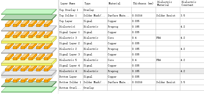
The layer stackup defines the sequence of dielectric, foil, and core materials in a PCB. Optimizing the stackup is critical for RF designs to enable proper isolation, shielding, and impedance control. Key factors in PCB stackup configuration include:
Layer Sequence
- Ground and power plane layers spaced through the stackup
- Signal layers interleaved between ground planes for isolation
- Surface layers for component placement
- Stackup symmetry aids thermal stability
Dielectric Selection
- Materials optimized for target frequency range
- Consistent dielectric constants and low loss tangents
- Tight thickness tolerances for impedance control
- High resin content improves signal integrity
Foil Types
- 1⁄2 oz to 2 oz copper foils standard
- Heavier copper used for power distribution
- Modified foil shapes enhance impendance control
- Surface roughness impacts high frequency loss
Core Thickness
- Thinner cores allow finer lines and spaces
- Thick cores provide mechanical rigidity
- Thermally conductive cores aid heat spreading
- Thin cores help minimize layer count
Plane Layers
- Solid reference planes for low impedance
- Power and ground planes decouple noise
- Flood unused areas on signal layers
- Planes surround critical traces
Layer Count
- 6 to 12 layer designs common for RF PCBs
- Higher layer counts offer routing flexibility
- May need 20+ layers for complex designs
- Each dielectric interface adds loss
Careful modeling during stackup design ensures the configuration supports the RF layout requirements before fabrication. Iteration is needed to optimize the stackup.
Dielectric Materials for RF PCBs
The dielectric material forms the insulating foundation of the PCB. For RF designs, properties like dielectric constant, loss tangent, moisture absorption and thermal conductivity need optimization. Common dielectric materials for high frequency PCBs include:
PTFE
- Lowest loss; dielectric constant around 2.1
- Expensive, poor thermal conductivity
- Common brands: Rogers RO4000 series
Ceramic Filled PTFE
- Mixes ceramic particles into PTFE resin
- Low loss, improved thermal performance
- Dielectric constants from 3 to 10
- Example: Rogers RO3000 series
Hydrocarbon Thermosets
- Offer cost/performance balance
- Dielectric constants between 3 and 4
- Moderate moisture absorption
- FR-4 suitable for lower microwave bands
Woven Glass Reinforced
- High resin content, moderate loss
- Low moisture absorption properties
- Balances cost and electrical performance
- Example: Megtron 6
Ceramic Substrates
- Alumina, aluminum nitride, glass ceramic
- Stable electrical properties
- High thermal conductivity
- Used for MMIC hybrid PCBs
Proper dielectric material selection enables RF PCBs to achieve target performance based on frequency range, loss, thermal and cost requirements.
Copper Foil for High Frequency PCBs
For RF PCBs, copper foil properties like weight, profile shape, surface roughness and plating process impact loss, current density and impedance control. Key considerations for foil specification include:
Weight
- 1⁄2 to 2 oz standard weights for signal layers
- 3 to 6+ oz used for power and ground planes
- Thicker copper lowers conductive losses
Profile Shape
- Standard rectangular cross-section foils widely used
- Modified shapes like trapezoidal improve impendance control
Surface Roughness
- Profile affects skin effect losses at high frequencies
- Very low profile foils preferred for microwave PCBs
- Double-treated foils offer cost/performance balance
Plating Process
- Standard subtractive etch removes unwanted copper
- Semi-additive builds up traces only where needed
- Fully-additive electroplates copper only on traces
Grain Structure
- Rolled copper grains impact foil strength
- Electrodeposited foils have finer grains
Bond Enhancement
- Chemical bonding improves adhesion
- Treatments like silane coating used
Solderability
- Hot air solder level (HASL) provides coatings
- OSP and ENIG also enhance solderability
Paying attention to foil properties ensures high conductivity, consistency and reliability needed in RF PCBs operating at up to millimeter wave frequencies.
key to achieving signal integrity for high frequency operation
During PCB layout, following RF design guidelines is key to achieving signal integrity for high frequency operation. Important considerations include:
Controlled Impedance
- Match trace widths and spacings to target impedance
- Minimize length discrepancies between differential pairs
- Use impedance calculators and field solvers to design traces
Isolation Techniques
- Enclose circuitry in ground planes to prevent coupling
- Separate noisy digital and sensitive analog sections
- Strategically place ground vias to isolate signals
Proper Grounding
- Connect all grounds to root plane using thermal reliefs
- Avoid ground loops
Efficient Power Distribution
- Decouple each power pin with localized capacitance
- Use multiple vias to deliver clean power to ICs
- Separate analog and digital power supplies
Minimal Right Angles
- Use 45 degree bends to reduce reflection losses
- Avoid stubs – route to vias directly without overshoot
Component Placement
- Place active devices before passive components
- Position interconnect-critical ICs close together
- Orient devices to optimize routing paths
Route for Constant Impedance
- Tapering maintains impedance through bends
- Length match critical traces like clocks or differentials
Applying these guidelines during layout helps RF PCBs achieve target functionality with maximum signal integrity.
Modeling and Simulation
With RF systems, the PCB layout significantly impacts performance and cannot be an afterthought. Advanced modeling and simulation techniques enable optimizing the board layout before fabrication to minimize field failures.
3D Electromagnetic Simulation
Full 3D EM analysis predicts signal behavior and identifies resonance risks. Field solvers like Ansys HFSS simulate propagation losses, coupling, radiation and gain insight into the RF board performance.
Thermal Modeling
Multiphysics solvers like Ansys Icepak model airflow and heat transfer to determine temperature profiles across PCBs when powered. This highlights hotspots needing heat sink optimization.
Power Integrity
Power delivery network modeling confirms clean power distribution to ICs. Identifies inrush risks, voltage drops, and decoupling needs.
Signal Integrity
Digital layouts are simulated to minimize noise coupling, reflections, timing issues. Important for high-speed data links.
Antenna Design
RF engineers can design and optimize integrated antennas for wireless using full-wave 3D EM solvers.
Manufacturing Analysis
Process variability modeling predicts impedance, resonances and performance deviations from nominal design to assess robustness.
Advanced modeling gives invaluable insight into RF PCB performance before committing to fabrication. While adding simulation time, this minimizes expensive re-spins, delays, and field failures.
Importance of Controlled Impedance
In RF PCBs, maintaining controlled impedance in routed traces is mandatory for proper signal transmission and to avoid reflections. Key factors include:
Impedance Matching
- Mismatched impedance causes signal reflections
- Noise, data errors, lower bandwidth
- Matched impedance allows maximum power transfer
Modeling Complexity
- Many factors impact trace impedance
- Dielectric constant, copper thickness, width, plane proximity
- Field solvers model complex geometries accurately
Narrow Tolerances
- Even small variations can cause mismatches
- Consistent line widths and dielectric constants needed
- Tight fabrication process control essential
Tuning Techniques
- Small variations can be tuned out in layout
- Length matching, minor width changes
-laser trimming of traces post-fab
Material Selection
- Dielectrics with low loss tangent, tight tolerances
- Thermally stable electrical properties
Layer Stackup
- Thin dielectrics enable fine features
- Signal layers spaced by ground planes
Routing Approach
- Plan controlled impedance layers first
- Define reference planes, then route signals
Achieving target impedance across PCB traces ensures matched terminations, allowing RF boards to deliver noise-free wireless communication at multi-GHz frequencies.
RF PCB Design Process
Successfully designing and implementing high frequency PCBs involves an integrated, iterative approach spanning schematic capture, analysis, layout, prototyping and testing.
Schematic Design
Create circuit schematics with proper RF components, interconnects and interfaces needed for the wireless, radar or communication functionality.
Stackup Definition
Select dielectric materials, conductor weights, layer count based on layout requirements, isolations needs and controlled impedance targets.
Layout – Component Placement
Strategically place ICs and discrete passives considering signal and thermal requirements. Group related components.
Layout – Routing
Route traces for controlled impedance, isolation between sections, minimal length discrepancies, and efficient grounding.
Modeling and Simulation
Run EM, thermal, power integrity, signal integrity, manufacturability simulations to verify performance. Iterate as needed.
Prototyping
Build prototypes for validation. May require several boards for RF modular evaluation, thermal testing etc.
Measurement and Tuning
Test boards for resonance, radiation, power consumption, modulation, data rates. Tune if needed through layout changes.
Release to Production
Finalize fabrication documentation after validating RF performance meets requirements through measurement.
Leveraging this integrated design flow enables RF PCBs to deliver the targeted functionality from initial concept to volume production.
Take a Quick Quote
Discover how our expertise can help with your next PCB project.