
Back to blog
What is EMI, EMS and EMC?

EMC Test
Electromagnetic compatibility (EMC) is a critical consideration in the design and manufacturing of electronic devices, especially on PCBs. This article aims to delve into the concepts of Electromagnetic Interference (EMI), Electromagnetic Susceptibility (EMS), and EMC, exploring their definitions, standards, testing methodologies, and implications in contemporary electronics.
What is EMI?
Electromagnetic Interference (EMI) refers to the disruption caused by electromagnetic energy emitted from electronic devices. This interference can adversely affect the performance of nearby electronic equipment, leading to malfunctions or data corruption. EMI sources include electric motors, radio transmitters, and even natural phenomena like lightning.
EMI Standards and Detection
EMI standards specify limits for electromagnetic emissions from electronic devices to ensure they do not interfere with other devices. Detection involves measuring emitted radiation across various frequencies and comparing them against regulatory thresholds. Techniques such as near-field scanning and spectrum analysis are employed during EMI testing to identify sources of interference.
Electromagnetic Phenomena and Testing
Common examples of EMI include screen distortion on TVs caused by nearby appliances like hair dryers, or audio disturbances when mobile phones are in use near speakers. In critical scenarios, EMI can disrupt medical equipment or communication systems, underscoring the need for rigorous testing and compliance with international standards.
What is Electromagnetic Susceptibility?
Electromagnetic Susceptibility (EMS) measures the sensitivity of electronic devices to external electromagnetic fields. Just as individuals vary in susceptibility to viruses, electronic devices differ in their resilience to EMI. Strong EMS ensures devices can operate reliably in diverse electromagnetic environments without performance degradation.
Understanding Immunity
EMS testing evaluates how well devices tolerate electromagnetic disturbances without malfunctioning. Strong immunity mitigates the risk of disruption from EMI, enhancing reliability and safety in applications ranging from consumer electronics to aerospace systems.
What is EMC?
EMC stands for Electromagnetic Compatibility. It refers to the ability of electronic and electrical systems, equipment, and devices to operate without generating excessive electromagnetic interference (EMI) that would interfere with other equipment in their vicinity, and without being affected by electromagnetic interference from other sources. In simpler terms, EMC ensures that electronic devices can coexist and operate correctly in the same electromagnetic environment without causing or suffering from disruptions.
Key Aspects of EMC:
- Emission Control: EMC involves managing and controlling the electromagnetic emissions from electronic devices. This includes ensuring that devices do not emit electromagnetic radiation above regulatory limits, which could interfere with the operation of nearby electronic equipment.
- Immunity: EMC also addresses the susceptibility of electronic devices to electromagnetic interference generated by other devices or external sources. Devices need to be designed to withstand reasonable levels of interference without malfunctioning.
- Regulatory Compliance: Most countries have regulatory standards and limits for EMC, which manufacturers must adhere to in order to market their products. Compliance typically involves testing devices for emissions and immunity according to specific standards such as those issued by the International Electrotechnical Commission (IEC) or the Federal Communications Commission (FCC) in the United States.
- Design Considerations: Achieving EMC requires careful consideration during the design phase of electronic products. Factors such as PCB layout, shielding, grounding, and component placement play crucial roles in minimizing emissions and enhancing immunity.
- Testing and Certification: Manufacturers conduct EMC testing on their products to ensure compliance with regulatory standards before market release. Testing typically involves measuring emissions across various frequencies and evaluating immunity to simulated electromagnetic interference.
Importance of EMC:
- Reliability: Ensures that electronic devices operate reliably without being affected by or causing interference in their operating environment.
- Compatibility: Facilitates the integration and interoperability of different electronic devices and systems in various applications and settings.
- Safety and Compliance: Protects against potential hazards and ensures that products meet legal requirements and safety standards regarding electromagnetic interference.
- Market Access: Compliance with EMC regulations is often mandatory for accessing global markets, demonstrating product reliability and quality assurance to customers and regulatory authorities.
In essence, EMC is fundamental in modern electronics to ensure the seamless operation and coexistence of electronic devices in an increasingly interconnected and electromagnetic environment. It combines technical design practices, regulatory standards, and testing methodologies to achieve reliable and interference-free electronic systems.
How PCB designers can improve designs with EMC, EMS, and EMI
EMC, EMS, and EMI Integration in PCB Design
PCB designers enhance the quality and reliability of their designs by integrating principles of Electromagnetic Compatibility (EMC), Electromagnetic Susceptibility (EMS), and Electromagnetic Interference (EMI). By meticulously planning PCB layouts, selecting appropriate components, and optimizing grounding and shielding techniques, designers can minimize electromagnetic emissions and susceptibility. This proactive approach not only ensures compliance with regulatory standards but also mitigates risks of interference, thereby improving overall product performance and longevity.
Optimizing Layout and Component Selection
Key strategies for achieving robust EMC, EMS, and EMI design include optimizing PCB layouts to reduce signal crosstalk and maintaining signal integrity through controlled impedance matching. Designers prioritize the placement of critical components to minimize noise coupling and interference susceptibility. Moreover, selecting components with documented EMC performance characteristics and integrating effective shielding measures contribute significantly to enhancing the PCB’s ability to operate reliably in diverse electromagnetic environments.
Testing and Validation
Rigorous testing and validation form essential phases of ensuring effective EMC, EMS, and EMI design in PCBs. Utilizing electromagnetic simulation tools allows designers to predict and mitigate potential issues early in the design phase. Subsequent EMC testing verifies compliance with regulatory standards and validates the PCB’s immunity to external electromagnetic disturbances. This iterative process of design, simulation, testing, and refinement ensures that PCBs not only meet performance requirements but also exceed expectations in reliability and compatibility across various operational scenarios.

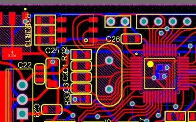
Electrical impedance
Mastering Impedance Control in PCB Design: Enhancing EMC and Mitigating EMI
Fine-tuning impedance lines is a critical step in PCB design, pivotal for reducing electromagnetic interference (EMI) and enhancing electromagnetic compatibility (EMC), thereby bolstering the board’s resilience to electromagnetic susceptibility (EMS). Here are some tried-and-true methods:
- PCB Layout Design:
- Impedance Control Areas: Designate specific zones in your PCB layout to meticulously regulate the impedance of crucial signal lines. These areas typically encompass high-speed signal paths or signals necessitating precise impedance matching.
- Signal Layer Placement: Ensuring vital signal routes are situated on appropriate layers, such as positioning signal lines on inner PCB layers to mitigate external interference and optimize impedance control.
- PCB Layer Stack Design:
- Optimal Layer Spacing and Dielectric Thickness: The spacing between PCB layers and the relative permittivity of the dielectric significantly affect signal line impedance. Strategically choosing layer spacing and dielectric thickness helps achieve desired impedance values.
- Stack-up Optimization: Fine-tuning the layer stack sequence (e.g., adjusting signal and ground plane positions) and selecting suitable interlayer dielectric materials (e.g., those with lower dielectric constants) aids in refining impedance lines.
- Utilization of PCB Design Tools:
- Employ professional PCB design software (e.g., Altium Designer, Cadence Allegro) offering calculation and simulation tools to accurately compute and adjust signal line impedance.
- These tools automate the process by calculating ideal impedance line layouts based on design parameters (e.g., layer stack, trace width, spacing, interlayer dielectric).
- Differential Signal Management:
- Impedance matching is particularly crucial for differential signals, ensuring uniform impedance throughout the signal path to uphold signal integrity and noise immunity.
- Employ differential pair techniques and verify consistent impedance matching across the entire signal path.
- Simulation and Validation:
- Pre-layout impedance simulation and validation are critical steps. Simulation tools simulate various layouts and parameters to assess their impact on impedance, ensuring design compliance with impedance requirements.
- Simulation aids in optimizing signal line layout and parameters to meet desired impedance control standards during PCB manufacturing.
In summary, through meticulous PCB layout design, layer stack optimization, utilization of advanced design tools for calculation and simulation, and rigorous impedance management techniques, engineers can effectively adjust and control impedance lines on PCBs. This enhances electromagnetic compatibility (EMC), immunity to electromagnetic interference (EMI), and resilience to electromagnetic susceptibility (EMS), aligning with Western preferences for thorough and precise technical approaches.
Conclusion
At Highleap Electronic, we specialize in producing high-quality PCBs by integrating advanced techniques for impedance control, ensuring robust electromagnetic compatibility (EMC) and mitigating electromagnetic interference (EMI). Our meticulous PCB layout designs, optimized layer stack configurations, and rigorous simulation-driven validation processes are tailored to meet stringent industry standards. By leveraging cutting-edge tools and expertise, we guarantee reliable performance and compliance with global EMC regulations, essential for seamless integration and operational reliability in diverse electronic applications. Trust Highleap Electronic for superior PCB solutions that exceed expectations in design integrity and electromagnetic performance.
FAQs
What role does signal integrity play in PCB design?
Signal integrity ensures that signals remain intact and free from distortion throughout their transmission paths on the PCB, contributing to overall system reliability and performance.
How does impedance affect signal quality in PCBs?
Impedance mismatches can lead to signal reflections and loss of signal integrity, impacting the functionality and reliability of electronic devices.
Why is differential signaling important in high-speed PCB design?
Differential signaling reduces electromagnetic interference and enhances noise immunity, crucial for maintaining signal integrity in high-speed data transmission.
What are some advanced methods for shielding PCBs against EMI?
Advanced shielding techniques include using conductive enclosures, shielding coatings, and strategic placement of shielding materials to minimize EMI effects.
How does PCB design impact compliance with global EMC regulations?
PCB design influences electromagnetic emissions and susceptibility levels, which must comply with international standards such as those set by the FCC (Federal Communications Commission) and IEC (International Electrotechnical Commission).

Related Articles
Analysis of Power Supply Noise in HF PCB Design Process
This comprehensive guide explores the complexities of power supply noise, its origins, and advanced techniques to mitigate its effects in high-frequency PCB designs.
Understanding Field-Effect Transistors (FETs) in PCB Design
Dive into the fundamentals of Field-Effect Transistors (FETs) and their critical role in PCB design.

Future Prospects and Challenges in Local Oscillator Development
Developing multi-function chips that integrate local oscillators(LOs) with other RF components, such as mixers, amplifiers, and filters, is an emerging trend.
Take a Quick Quote