
Back to blog
Understanding Crystal Oscillators and Their PCB Layout
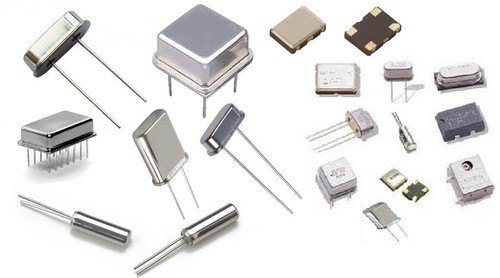
Crystal oscillator design layout on PCB board
As the heart of the digital circuit, the crystal oscillator affects the stability of the entire system. The choice of the system crystal oscillator determines the success or failure of the digital circuit.
Since there is a quartz crystal inside the crystal oscillator, it is easy to cause the crystal oscillator to stop vibrating due to external impact, etc., so the reliable installation of the crystal oscillator must be considered when designing the circuit, and its location should not be close to the board edge, equipment shell, etc. . When laying out the crystal oscillator on the PCB, you usually pay attention to the following points:
- The crystal oscillator cannot be too close to the edge of the board, and the shell of the crystal oscillator must be grounded, otherwise it will easily cause the crystal oscillator to radiate noise.This is especially important to pay attention to when designing the board. Grounding the shell can prevent the crystal oscillator from radiating outward, and can also shield the crystal oscillator from interference from external signals. If it must be arranged on the edge of the PCB, you can place another GND line next to the crystal oscillator printed line, and drill holes at a certain distance on the ground line to surround the crystal oscillator.
- Signal lines cannot be laid under the crystal oscillator, otherwise it will easily cause the signal lines to couple with harmonic noise from the crystal oscillator.Ensure that the ground is completely paved and do not route wiring within 300mil of the crystal oscillator. This can prevent the crystal oscillator from interfering with the performance of other wiring, components and layers.
- If the filter device is placed under the crystal oscillator, and the filter capacitor and matching resistor are not arranged according to the signal flow direction, the filtering effect of the filter will be deteriorated.The coupling capacitors should be placed as close as possible to the power pins of the crystal oscillator in descending order of capacitance value according to the direction of power flow.
- The wiring of the clock signal should be as short as possible, with a wider line width, and find a balance between wiring length and distance from heat sources.The following layout is taken as an example.
PCB & PCBA quick quote
Related Articles

PCB SMD Components and How to Identify Them
[pac_divi_table_of_contents title="On this article" default_state="closed" included_headings="off|on|on|off|off|off" exclude_headings_by_class="on" active_link_highlight="on" level_markers_3="icons" title_container_padding="10px|15px|10px|15px|true|false"...

Lead vs. Lead-free Solder: A Comprehensive Comparison
[pac_divi_table_of_contents title="On this article" default_state="closed" included_headings="off|on|on|off|off|off" exclude_headings_by_class="on" active_link_highlight="on" level_markers_3="icons" title_container_padding="10px|15px|10px|15px|true|false"...

Lead-Free PCB : Essential Considerations and Best Practices
[pac_divi_table_of_contents title="On this article" default_state="closed" included_headings="off|on|on|off|off|off" exclude_headings_by_class="on" active_link_highlight="on" level_markers_3="icons" title_container_padding="10px|15px|10px|15px|true|false"...

Choosing the Best Copper Clad Laminate : A Practical Guide
[pac_divi_table_of_contents title="On this article" default_state="closed" included_headings="off|on|on|off|off|off" exclude_headings_by_class="on" active_link_highlight="on" level_markers_3="icons" title_container_padding="10px|15px|10px|15px|true|false"...
Take a Quick Quote