
Back to blog
Lead-Free PCB : Essential Considerations and Best Practices

In the dynamic landscape of electronics manufacturing, the advent of lead-free printed circuit boards (PCBs) has emerged as a pivotal development. These PCBs, devoid of lead-based solder, have revolutionized the industry by offering a safer, more environmentally sustainable alternative. From consumer electronics to industrial applications, the adoption of lead-free PCBs has reshaped the way electronic devices are designed and manufactured.
The Transition to Lead-Free PCBs
The transition to lead-free PCBs was driven by regulatory initiatives such as the Restriction of Hazardous Substances Directive (RoHS). Enacted in 2006 by the European Union (EU), RoHS mandates the elimination of hazardous substances, including lead, from electrical and electronic equipment. This directive has had a profound impact on the electronics industry, spurring innovation and reshaping manufacturing practices worldwide.
Advantages of Lead-Free PCBs
Lead-free PCBs offer several key advantages:
- Environmental Impact: Lead-free PCBs are environmentally friendly, reducing the impact of electronic waste on the environment. By eliminating lead, these PCBs contribute to a cleaner and safer manufacturing process.
- Health Benefits: Lead is a known health hazard, particularly in the manufacturing environment. Lead-free PCBs help protect workers and consumers from the harmful effects of lead exposure, promoting a safer working environment.
- Compliance: Compliance with RoHS and other environmental regulations is critical for manufacturers. By using lead-free PCBs, companies can ensure compliance with these regulations and avoid costly penalties.
- Improved Reliability: Lead-free solder offers improved mechanical and thermal properties compared to lead-based solder. This results in more reliable connections and longer-lasting electronic devices.
- Global Acceptance: Lead-free PCBs are now widely accepted and preferred in global markets. Manufacturers that use lead-free solder can access a broader customer base and expand their market reach.
RoHS Compliance and PCB Manufacturing
The Restriction of Hazardous Substances Directive (RoHS) sets stringent standards for the use of hazardous substances in electrical and electronic equipment (EEE). PCB manufacturing plays a crucial role in achieving RoHS compliance, as PCBs are integral components of most electronic devices. Understanding RoHS requirements and working with experienced PCB manufacturers is essential for companies seeking to meet these environmental standards.
RoHS Requirements for PCBs
RoHS restricts the use of six hazardous substances in EEE:
- Lead (Pb)
- Mercury (Hg)
- Cadmium (Cd)
- Hexavalent chromium (Cr6+)
- Polybrominated biphenyls (PBB)
- Polybrominated diphenyl ethers (PBDE)
For PCB manufacturers, the most significant impact of RoHS is the restriction of lead in solder and finishes. Lead-free solder and surface finishes are now standard in RoHS-compliant PCB manufacturing processes.
Selecting RoHS-Compliant Materials
PCB manufacturers must carefully select materials that comply with RoHS regulations. This includes lead-free solder, surface finishes, and laminates. Lead-free solder alloys, such as SAC (tin-silver-copper) and SnAgCu (tin-silver-copper), are commonly used in RoHS-compliant PCBs. These alloys have properties similar to traditional lead-based solders but without the environmental and health risks associated with lead.
Surface finishes are also crucial for RoHS compliance. Common RoHS-compliant surface finishes include:
- Electroless Nickel Immersion Gold (ENIG)
- Immersion Silver
- Organic Solderability Preservatives (OSP)
- Immersion Tin
By selecting the right solder and surface finishes, PCB manufacturers can ensure that their products meet RoHS requirements while maintaining high performance and reliability.
Partnering with Experienced PCB Manufacturers
Achieving RoHS compliance requires expertise in PCB manufacturing and materials selection. Experienced PCB manufacturers understand the complexities of RoHS regulations and can guide companies through the process of selecting RoHS-compliant materials and processes.
By partnering with experienced PCB manufacturers, companies can:
- Ensure compliance with RoHS regulations
- Reduce the risk of non-compliance and associated penalties
- Improve the environmental sustainability of their products
- Enhance their reputation as environmentally responsible companies
RoHS compliance is a critical aspect of PCB manufacturing, requiring careful selection of materials and processes to meet stringent environmental standards. By working with experienced PCB manufacturers, companies can navigate the complexities of RoHS regulations and contribute to a more sustainable future for electronics manufacturing.
Comparing Leaded vs. Lead-Free Solder Paste in PCB Manufacturing
Solder paste is a critical component in PCB manufacturing, and the choice between leaded and lead-free solder pastes can have significant implications for the final product. Here, we’ll compare the two types of solder paste in terms of their properties, application, and impact on PCB assembly.
Leaded Solder Paste
Leaded solder paste typically consists of a mixture of tin and lead, with common ratios being 60/40 or 63/37. This type of solder paste has a lower melting point, typically around 361°F, making it easier to work with and quicker to bring to a working temperature. Leaded solder paste also tends to flow well, which can result in smooth, shiny solder joints that are visually appealing.
However, the use of leaded solder paste comes with significant environmental and health risks. Lead is a toxic substance that can be harmful to both humans and the environment. As a result, the use of leaded solder paste is regulated, and it should only be used when permitted by regulatory agencies. Proper disposal of leaded solder paste is also essential to prevent environmental contamination.
Lead-Free Solder Paste
Lead-free solder paste is an alternative to leaded solder paste that complies with RoHS regulations. It typically contains a mixture of tin, silver, copper, and other elements, with a higher melting point of around 422°F. While the higher melting point of lead-free solder paste may require changes in soldering practices, joints soldered with lead-free solder paste have been shown to be reliable.
One of the challenges of lead-free solder paste is that it does not wet as well as leaded solder paste, which can result in differences in the appearance of solder joints. Despite this, lead-free solder paste can still produce strong mechanical joints, making it suitable for a wide range of PCB applications.
Other Factors to Consider
In addition to solder paste composition, several other factors can affect the reliability of soldered joints in PCB assembly. These include temperature, vibration, tin whisker formation, preheating time, throughput, and operator skill levels. Proper consideration of these factors, along with the use of high-quality solder paste, is essential for manufacturing dependable PCBs.
Overall, the choice between leaded and lead-free solder paste in PCB manufacturing depends on a variety of factors, including regulatory compliance, environmental impact, and solder joint quality. While leaded solder paste may offer certain advantages in terms of ease of use and solder joint appearance, lead-free solder paste is the environmentally responsible choice and is required for RoHS compliance. By working with a PCB manufacturer that has extensive experience in RoHS material compliance, companies can ensure that their PCBs are manufactured to the highest standards of quality and environmental responsibility.
When the project moves from research to an RFQ, review PCB prototype review and circuit board cost review so the material, process, and inspection requirements stay aligned.
Lead or Lead-free: Which One is Better to Use?
It’s true that the choice between leaded and lead-free solder is not a simple one, and it depends on various factors such as environmental regulations, component compatibility, and application requirements. Here’s a more detailed comparison to help you make an informed decision:
Environmental Impact:
- Leaded solder is known to be harmful to the environment and human health, which is why many countries have banned or restricted its use in consumer electronics.
- Lead-free solder, on the other hand, is considered more environmentally friendly and complies with regulations such as the RoHS directive.
Component Compatibility:
- Lead-free solder typically has a higher melting point than leaded solder, which can affect the compatibility with components that are sensitive to heat.
- Some components, especially those with lower dielectric constants, may be more vulnerable to damage from the higher temperatures required for lead-free soldering.
Corrosion Resistance:
- Lead-free solder generally exhibits higher corrosion resistance compared to leaded solder, making it a better choice for applications where the circuit boards are exposed to high-corrosion environments.
Regulatory Compliance:
- As mentioned, both the United States and the European Union have implemented regulations restricting the use of lead in electronics, making lead-free solder the preferred choice for compliance with these regulations.
Overall, while leaded solder may have certain advantages in terms of ease of use and lower melting point, the environmental and health concerns associated with lead make lead-free solder the more sustainable choice. When choosing between the two, it’s essential to consider your specific application requirements and environmental regulations to make the best decision for your PCBs.
Effects of Lead and Lead-free Solder on Different Types of Soldering
Soldering is a critical process in PCB manufacturing, and the choice between leaded and lead-free solder can significantly impact the quality and performance of the final product. Here’s a more detailed look at how lead and lead-free solder affect different types of soldering processes:
Wave Soldering:
- Wave soldering is a common method for soldering through-hole components onto a PCB.
- Lead-free solder typically requires higher temperatures compared to leaded solder, which can affect the wave soldering process.
- Proper control of soldering parameters, such as temperature and conveyor speed, is crucial to ensure that components are soldered correctly and without damage.
Reflow Soldering:
- Reflow soldering is used for surface-mount components and involves heating the entire PCB to reflow the solder paste.
- Lead-free solder has a higher melting point, which requires a longer reflow process and higher temperatures compared to leaded solder.
- Proper thermal profiling is essential to ensure that the solder joints are formed correctly and that components are not damaged due to overheating.
Selective Soldering:
- Selective soldering is used to solder through-hole components in areas where wave soldering is not feasible.
- Lead-free solder may require adjustments to the selective soldering process, such as higher preheat temperatures and longer dwell times, to ensure proper soldering.
Hand Soldering:
- Hand soldering is often used for rework or for soldering components that cannot be soldered using automated methods.
- Lead-free solder may require more skill and experience to work with due to its higher melting point and different wetting characteristics compared to leaded solder.
Impact on PCB Quality:
- The choice between leaded and lead-free solder can impact the quality of solder joints and the overall reliability of the PCB.
- Lead-free solder joints may be more prone to issues such as cold solder joints or insufficient wetting if not soldered correctly.
- Proper training of operators and adherence to soldering standards are essential to ensure that PCBs are soldered correctly and meet quality requirements.
Overall, while lead-free solder offers environmental and health benefits, it requires careful consideration and proper implementation to ensure that it does not compromise the quality and reliability of PCBs. Manufacturers must carefully evaluate their soldering processes and consider factors such as component compatibility, regulatory requirements, and soldering standards when choosing between leaded and lead-free solder.
Conclusion
The adoption of lead-free PCBs marks a significant milestone in the evolution of electronics manufacturing. By adopting lead-free solder, manufacturers can reduce their environmental impact, enhance product reliability, and comply with regulatory standards. Although the transition may necessitate adjustments, the long-term advantages far outweigh the challenges. Lead-free PCBs represent more than just a technological advancement; they signify the industry’s dedication to sustainability and innovation. As the electronics sector continues to progress, lead-free PCBs will undoubtedly play a pivotal role in shaping its future.
PCB & PCBA Quick Quote
Related Articles
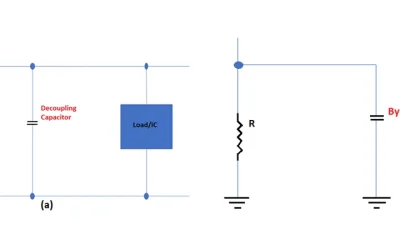
Bypass vs Decoupling Capacitor: Understanding Their Distinct Roles in PCB Design
Learn the critical differences between bypass and decoupling capacitors in PCB design, their applications, and proper placement strategies.
Tantalum Capacitors: Complete Guide to Selection, Performance, and PCB Implementation
Comprehensive guide to tantalum capacitors covering types, electrical characteristics, PCB design rules, and selection criteria for engineers.
MLCC Explained: Definition, Types & Selection Guide in PCBA
Comprehensive guide to MLCC selection, types, parameters, and applications in PCB design. Learn how to choose the right ceramic capacitor.