Back to blog
Understanding Field-Effect Transistors (FETs) in PCB Design

Field Effect Transistors+FET
Introduction
Field-Effect Transistors (FETs) are crucial components in modern electronics, serving as the backbone of various integrated circuits. Since Julius Edgar Lilienfeld first conceptualized the FET in 1926, these transistors have undergone significant advancements, becoming integral to technological innovation. In today’s technology-driven world, understanding FETs is essential for any PCB designer aiming to create efficient and effective electronic circuits.
This extensive guide delves into the fundamentals, types, operational principles, and applications of FETs, providing professional insights and unique content that will benefit advanced PCB designers.
Understanding Field-Effect Transistors
Basic Structure and Operation
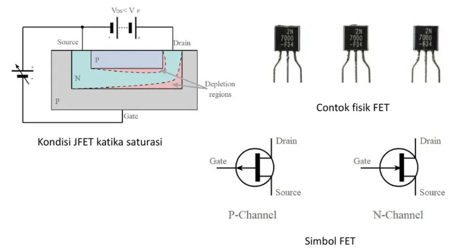
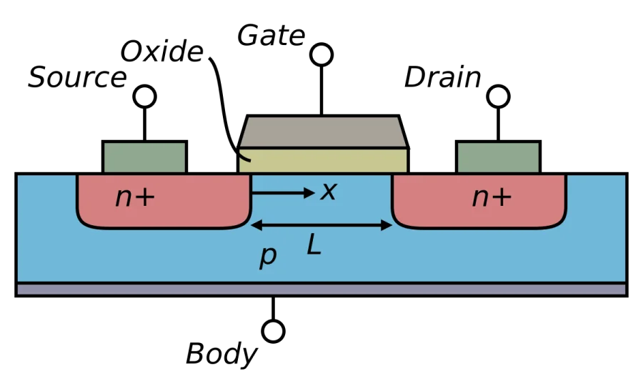
A Field Effect Transistor (FET) is a three-terminal semiconductor device that controls current flow using an electric field. The primary components of a FET are the source, drain, and gate. The source is the terminal where the current enters, the drain is where the current exits, and the gate controls the current flow by modulating the electric field within the channel between the source and drain.
Unlike Bipolar Junction Transistors (BJTs), which control current flow through charge carrier injection, FETs operate by varying the conductivity of a semiconductor channel using an electric field. This key difference endows FETs with high input impedance, low power consumption, and excellent high-frequency performance.
Types of FETs
FETs are categorized into several types, each with specific characteristics and applications:
- Junction Field-Effect Transistor (JFET)
- N-Channel JFET: Uses N-type semiconductor material for the channel.
- P-Channel JFET: Uses P-type semiconductor material for the channel.
- Operation: JFETs control current flow through a semiconductor channel using an electric field applied across a PN junction.
- Metal-Oxide-Semiconductor Field-Effect Transistor (MOSFET)
- N-Channel MOSFET: The channel is formed in N-type semiconductor material.
- P-Channel MOSFET: The channel is formed in P-type semiconductor material.
- Operation: MOSFETs operate by applying a voltage to a metal gate, creating an electric field that controls the flow of charge carriers between the source and drain terminals.
- Insulated Gate Bipolar Transistor (IGBT)
- Structure: Combines features of MOSFETs and BJTs, with a gate like a MOSFET and conductivity modulation similar to a BJT.
- Operation: Used for high-power applications, providing high current and voltage capabilities.
- High Electron Mobility Transistor (HEMT)
- Characteristics: Known for high electron mobility and low noise, suitable for high-frequency applications.
- Applications: Used in satellite communications, radar systems, and cellular networks.
- Gallium Nitride Field-Effect Transistor (GaN FET)
- Characteristics: Known for high power density and efficiency.
- Applications: Used in power electronics applications such as electric vehicle charging, renewable energy systems, and wireless power transfer.
Each type of FET has unique attributes that make it suitable for specific applications. Selecting the appropriate FET type is crucial for optimizing performance and ensuring reliability in your circuit design.

Field Effect Transistors
Detailed Examination of FET Characteristics
Key Specifications
Understanding FET specifications is essential for ensuring optimal performance in your applications. Key parameters include:
- Drain-Source Breakdown Voltage (BVDS): Maximum voltage that can be applied between the drain and source without causing breakdown.
- Gate-Source Voltage (VGS) Range: Voltage range required to control the FET’s conductivity.
- Drain Current (ID): Maximum current through the drain when the FET is fully on.
- On-Resistance (RDS(on)): Resistance of the FET when it is on, affecting power dissipation and efficiency.
- Gate Threshold Voltage (VGS(th)): Minimum voltage needed at the gate to turn the FET on.
- Capacitances (Ciss, Coss, Crss): Affect high-frequency performance and switching speeds.
Advanced Characteristics
- Thermal Resistance (RθJC, RθJA): Indicates the FET’s ability to dissipate heat, crucial for high-power applications.
- Switching Speed: Influenced by gate capacitance, important for high-frequency and digital applications.
- Safe Operating Area (SOA): Defines the limits within which the FET can operate without damage.
Designing FET Circuits: Sharing My Expertise
Biasing Techniques
Over the years, I’ve found that getting the biasing right is crucial for FET operation. Here are some methods that have worked well for me:
-
- Voltage Divider Biasing: This technique involves using a resistor network to set a stable gate voltage. It’s reliable and provides good control over the gate voltage, ensuring consistent operation.
- Self-Biasing: By using feedback from the source, you can stabilize the operating point. This method is particularly useful in amplifier circuits where stability is key.
- Fixed Biasing: Applying a direct voltage source to the gate can be straightforward and effective, especially in simpler circuits where precise control over the gate voltage is needed.
Each method has its unique advantages, and selecting the right one depends on the specific requirements of your circuit. It’s always a good idea to experiment with these techniques to see which one best suits your needs.
Load Line Analysis
In my experience, load line analysis is indispensable when designing FET circuits. By plotting the output characteristics and the load line on the same graph, you can easily determine the FET’s operating point. This step is essential for ensuring your amplifiers and other analog circuits perform optimally. It helps you visualize how the FET will behave under different operating conditions and allows you to make informed adjustments.
Impedance Matching
Impedance matching is another critical aspect. Understanding both the input and output impedance of FETs is crucial for optimizing signal transfer and minimizing losses. Proper impedance matching ensures that your circuit stages interconnect efficiently, which can significantly enhance performance. I’ve found that spending time on this step pays off in the overall efficiency and functionality of the circuit.
Protection Circuits
Lastly, don’t overlook the importance of protection circuits. Implementing Zener diodes and transient voltage suppressors can prevent damage from overvoltage and overcurrent conditions. This not only enhances the reliability of your circuits but also extends their longevity. In my projects, incorporating these protection measures has saved a lot of time and resources by avoiding potential failures and ensuring stable operation.
By integrating these practices into your FET circuit designs, you can achieve more robust and reliable results. It’s about finding the right balance and fine-tuning each aspect to suit your specific application.

Field Effect Transistors
Applications of FETs
Amplifiers
FETs are ideal for amplifier circuits due to their high input impedance and low noise. Common configurations include:
- Common Source Amplifier: Provides high voltage gain.
- Common Drain (Source Follower) Amplifier: Offers high input impedance and unity voltage gain.
- Common Gate Amplifier: Used for high-frequency applications.
Switches
FETs are preferred for switching applications due to their fast switching speeds and low on-resistance. They are widely used in digital logic circuits, power supplies, and motor controllers.
Oscillators
FETs are used to design oscillators for generating stable and precise frequency signals, essential in RF circuits, signal generators, and clocks.
Voltage Regulators
FETs are crucial in both linear and switching voltage regulators, providing stable and efficient power to electronic circuits by maintaining constant output voltage despite variations in input voltage and load conditions.
Digital Logic Circuits
Complementary MOSFET (CMOS) technology, which uses both N-channel and P-channel MOSFETs, creates logic gates with low power consumption and high noise immunity, forming the basis of modern digital circuits.
Conclusion
Field-Effect Transistors (FETs) are fundamental to modern electronics, offering unique advantages such as high input impedance, low power consumption, and rapid switching capabilities. Their diverse types and characteristics make them suitable for a wide range of applications, from amplifiers and switches to high-frequency and power electronics.
PCBs provide the physical platform and necessary connectivity for integrating FETs with other electronic components. The layout and design of the PCB, including trace routing and thermal management, significantly impact the performance of FETs. Proper PCB design ensures that FETs operate within their optimal parameters, reducing the risk of overheating and signal interference. Additionally, the PCB material selection and layer configuration play a pivotal role in supporting the high-frequency performance of FETs, making PCBs an indispensable part of modern electronic systems that utilize FET technology.
For professional PCB designers, a deep understanding of FETs and their operational principles is crucial for creating efficient and reliable electronic circuits. By staying informed about the latest developments in FET technology and applying advanced design techniques, designers can harness the full potential of these versatile devices to innovate and excel in the ever-evolving field of electronics.
FAQ: Advanced Field-Effect Transistors (FETs)
1. How do Field-Effect Transistors (FETs) compare to other transistors in terms of thermal management?
FETs, particularly power FETs like MOSFETs and IGBTs, require effective thermal management due to their high power density. Unlike BJTs, which dissipate power more evenly, FETs can generate significant localized heat. Advanced cooling techniques, such as heat sinks, thermal pads, and even liquid cooling in high-power applications, are often necessary to maintain performance and prevent thermal runaway.
2. What role do FETs play in high-frequency applications, and how do they achieve high performance in such scenarios?
FETs are preferred in high-frequency applications due to their fast switching speeds and low capacitance. Devices like High Electron Mobility Transistors (HEMTs) and Gallium Nitride (GaN) FETs excel in these applications. Their high electron mobility and low parasitic capacitance enable efficient operation at microwave and millimeter-wave frequencies, making them ideal for RF amplifiers, satellite communications, and radar systems.
3. Can you explain the significance of gate drive circuits in FET operation, particularly for high-power applications?
Gate drive circuits are crucial for controlling the switching performance of FETs, especially in high-power applications. These circuits must provide the necessary voltage and current to switch the FET on and off rapidly while minimizing switching losses. In high-power scenarios, gate drivers also need to handle the high gate charge and ensure synchronization in multiple FET setups to avoid shoot-through and other issues.
4. What advancements in material science are influencing the development of next-generation FETs?
Recent advancements in material science, such as the development of silicon carbide (SiC) and gallium nitride (GaN) materials, are significantly impacting the evolution of FET technology. SiC FETs offer higher thermal conductivity and breakdown voltage, making them suitable for high-temperature and high-voltage applications. GaN FETs, on the other hand, provide higher electron mobility and efficiency, ideal for high-frequency and power switching applications.
5. How do FETs contribute to the efficiency of renewable energy systems, particularly in solar inverters and electric vehicle chargers?
FETs, particularly SiC and GaN types, enhance the efficiency of renewable energy systems by enabling higher switching frequencies and lower conduction losses. In solar inverters, these FETs help convert DC to AC with minimal power loss, improving overall system efficiency. In electric vehicle chargers, they support faster charging rates and better thermal management, making the charging process more efficient and reliable.
Related Articles
Understanding Silkscreen on PCB: A Comprehensive Guide for PCB Manufacturers
We will dive deep into the world of PCB silkscreen, exploring its significance, printing methods, design considerations, and much more.
What is the use of decoupling capacitors in PCB?
Decoupling capacitors, also known as bypass capacitors, are used to filter noise from power lines and stabilize voltage levels on ICs.
What is the Meaning of Schematic Diagram?
Utilize hierarchical Schematic Diagrams to manage complex designs by breaking them into functional blocks, simplifying the overall structure.
Take a Quick Quote


