
Back to blog
What is the Meaning of Schematic Diagram?

Partial schematic diagram of gas alarm
A schematic diagram is the starting point of any PCB design handoff—it captures circuit intent and connectivity so your layout, BOM sourcing, and assembly documentation stay aligned. When you’re moving from design to hardware, a clean schematic also speeds up quoting and reduces back-and-forth with your supplier, whether you need bare board fabrication or SMT PCB assembly.
This guide focuses on the practical side of schematics: how to structure them for fast review, how to avoid common errors that lead to PCB respins, and how to prepare manufacturing-ready deliverables—from prototype runs to volume builds.
Understanding Schematic Diagrams
What is a Schematic Diagram?
A schematic diagram is a logical representation of an electrical circuit. It uses standardized symbols for components and nets to show how signals and power connect. Unlike a PCB layout (which shows physical placement and routing), a schematic emphasizes functional relationships—making design review, debugging, and production handoff far more efficient.
Importance of Schematic Diagrams
Schematic diagrams matter because they reduce ambiguity across the entire build process:
- Clarity: They organize complex circuits into readable functional blocks, so reviewers can verify intent quickly.
- Communication: They act as a shared reference between engineering, procurement, and manufacturing—reducing interpretation errors.
- Documentation: They preserve design intent for revisions, maintenance, and future upgrades, especially when teams change over time.
- Debugging: They make it easier to trace signal paths, validate power rails, and pinpoint issues before layout and assembly.

Smart fingerprint lock control board schematic (example)
Standards for Schematic Symbols
Schematic symbols are standardized globally to ensure consistency and understanding across different regions and industries. The primary standards are:
IEC 60617:The International Electrotechnical Commission (IEC) 60617 standard provides a comprehensive set of symbols for electrical and electronic components. It includes over 1750 symbols, ensuring detailed and accurate representation.
ANSI Y32:The American National Standards Institute (ANSI) Y32 standard, initially used for aircraft applications, has been adapted for general use. It aligns closely with IEC standards, ensuring global compatibility.
Common Schematic Symbols
Understanding common schematic symbols is essential for reading and creating diagrams. Here are a few examples:
-
- Resistors: Represented by a zigzag line or a rectangle.
- Capacitors: Depicted as parallel lines (for non-polarized) or a line and a curve (for polarized).
- Inductors: Shown as a series of loops or a rectangle with lines.
- Diodes: Represented by a triangle pointing to a line.
- Transistors: Depicted with arrows indicating the flow of current.
- Integrated Circuits (ICs): Shown as rectangles with multiple pins.

Common Schematic Symbols
Creating a Schematic Diagram
Creating a schematic diagram involves several steps, each requiring attention to detail and a clear understanding of the circuit. Here’s a step-by-step guide:
1. Define the Circuit Requirements
Before starting the schematic, outline the circuit’s functionality, components, and specifications. This ensures that the diagram will meet the design objectives.
2. Choose the Right Tools
Use advanced PCB design software, such as Altium Designer, Eagle, or KiCad, to create your schematic diagrams. These tools provide extensive libraries of symbols and automated features to simplify the process.
3. Generate Symbols
Create symbols for each component, ensuring they conform to the standard conventions. Include essential attributes like pin numbers, reference designators, and values.
4. Place Components
Arrange the symbols logically, grouping related components together. Place inputs on the left and outputs on the right to maintain a clear signal flow.
5. Draw Connections
Use lines to connect the components, representing the electrical connections. Ensure that lines intersecting at a junction have a node, indicating a connection.
6. Add Attributes
Include attributes for each component, such as resistance values for resistors, capacitance for capacitors, and voltage ratings for ICs. This information is crucial for selecting the right components during manufacturing.
7. Verify the Diagram
Double-check the schematic for errors, ensuring all connections are correct and all components are properly labeled. Use simulation tools to validate the circuit’s functionality.

Partial schematic diagram of oximeter
Best Practices for Drawing Schematic Diagrams
Adhering to best practices in schematic creation improves readability, review efficiency, and manufacturing handoff. Use standardized symbols (IEC/ANSI) consistently, and label every component with clear reference designators and values. Organize the design into functional blocks (power, MCU, analog, I/O), keep signal flow consistent (left-to-right, top-to-bottom where practical), and use meaningful net names (e.g., 3V3, 5V0, I2C_SCL, USB_D+). Minimize unnecessary wire crossings by using net labels and connectors, and include key notes directly on the schematic (polarity, connector pinout expectations, and any safety/creepage requirements).
For designs with high-speed or sensitive signals, the schematic should also capture design intent for layout and verification—such as interface requirements, differential-pair identification, and any stack-up or routing constraints that impact controlled-impedance requirements. Before moving to PCB layout, run ERC, validate pin mapping and power rails, and generate a netlist as a cross-check so the layout matches the schematic. If the circuit is performance-critical (power, analog, RF, high-speed I/O), simulation can be used to validate key blocks before prototyping.
Reading and Interpreting Schematic Diagrams
To effectively read and interpret schematic diagrams, follow these steps:
1. Identify the Components
Start by identifying the components and their symbols. Familiarize yourself with the reference designators and attributes.
2. Understand the Connections
Trace the lines connecting the components, understanding how signals flow through the circuit. Look for nodes indicating connections and pay attention to the orientation of polarized components.
3. Analyze the Functionality
Consider the circuit’s purpose and how the components work together to achieve it. Use the attributes to understand the operational parameters and requirements.
4. Check for Anomalies
Look for any discrepancies or potential issues, such as missing connections, incorrect values, or conflicting attributes. Verify the schematic against the design requirements and specifications.
Production-Ready Quote Checklist (For Accurate Pricing)
To receive an accurate and fast quote for PCB fabrication or PCBA/turnkey, please include the information below. Requests with complete files are prioritized and get the quickest turnaround.
For PCB Fabrication (Bare Board)
- Board size (L × W) and layer count
- Material / Tg requirement (or confirm standard FR-4)
- Finished copper thickness and board thickness
- Surface finish (ENIG / HASL / OSP, etc.)
- Solder mask color / silkscreen color (if required)
- Quantity and target lead time
- Gerber/ODB++ + drill files (or let us know your CAD format)
For PCBA / Turnkey Assembly
- BOM with Manufacturer Part Numbers (MPNs) and approved alternates (if allowed)
- Pick & Place / Centroid file (XY)
- Assembly drawing (polarity, orientation, special notes)
- Programming needs (if any) and functional test expectations (if available)
- Quantity per build (prototype vs. pilot vs. mass production)
If you’re not sure about any item above, send what you have—our engineers will reply with the minimum set needed to proceed.
Conclusion
A schematic diagram is more than a drawing—it’s the blueprint that determines whether your PCB can be built reliably and repeatedly. When your schematic is clear, correctly annotated, and reviewed (ERC + human review), you reduce errors, shorten layout time, and avoid costly PCB respins.
If you’re ready to manufacture, use the checklist above and submit your files for pricing. Quotes are fastest when Gerber/ODB++ (or CAD export) and a complete BOM (with MPNs) are included.
FAQs about Schematic Diagrams
1. What is the primary difference between a schematic diagram and a wiring diagram?
A schematic diagram shows the functional connections between components using standardized symbols, while a wiring diagram depicts the physical layout and connections of the components in a circuit.
2. How do schematic symbols differ between IEC and ANSI standards?
IEC symbols are more universally recognized and used globally, while ANSI symbols were initially developed for aircraft applications in the United States but have since been aligned with IEC standards.
3. Why is it important to include attributes like resistance, capacitance, and voltage in schematic diagrams?
Including these attributes ensures that the correct components are selected during manufacturing, and helps in understanding the operational parameters of the circuit.
4. How can hierarchical schematics simplify complex circuit designs?
Hierarchical schematics break down complex designs into functional blocks, making it easier to manage, understand, and troubleshoot each section of the circuit.
5. What role does simulation play in the schematic design process?
Simulation allows designers to test and analyze the circuit’s performance virtually, identifying potential issues and optimizing the design before moving to the physical layout stage.
Get a Free PCB & PCBA Quote

Recommended Posts
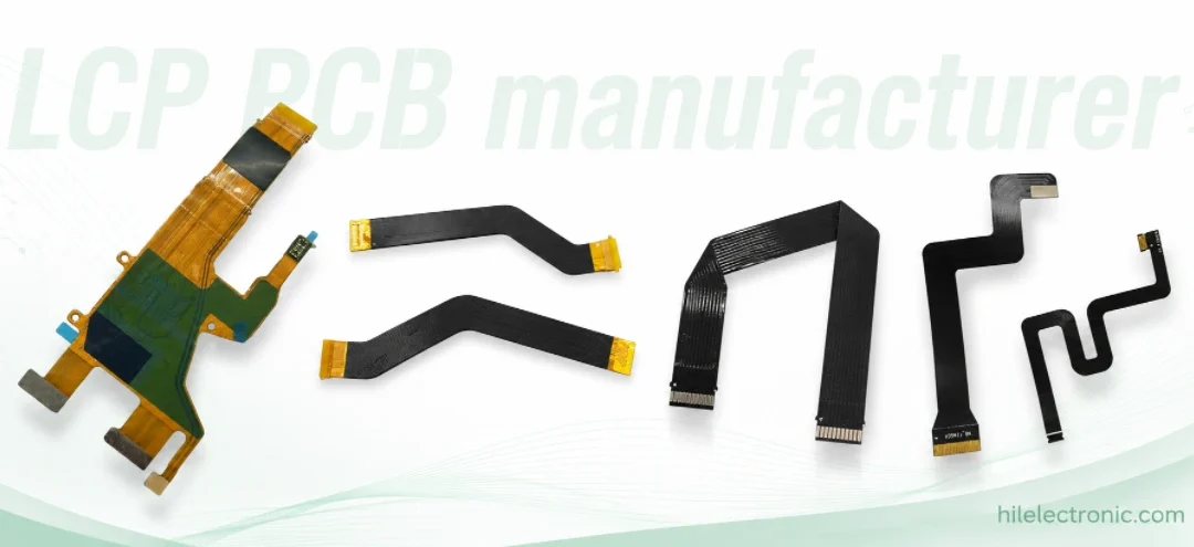
LCP PCB Manufacturer for High-Frequency and Compact Electronic Products
The phrase “LCP PCB manufacturer” covers several very...
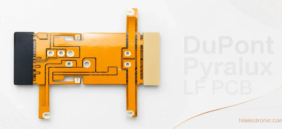
DuPont Pyralux LF PCB Manufacturing for Flexible Circuit Projects
A Pyralux LF flex circuit should be quoted from its...
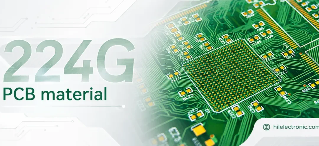
224G PCB Material Selection for Manufacturable PAM4 Channels
A 224G PCB request becomes actionable only when the...
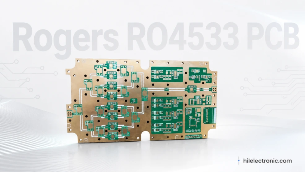
Rogers RO4533 PCB Manufacturing for Cost-Sensitive RF Products
RO4533 should be handled as a grade-specific commercial RF...
How to get a quote for PCBs
Let us run DFM/DFA analysis for you and get back to you with a report.
You can upload your files securely through our website.
We require the following information in order to give you a quote:
-
- Gerber, ODB++, or .pcb, spec.
- BOM list if you require assembly
- Quantity
- Turn time
In addition to PCB manufacturing, we offer a comprehensive range of electronic services, including PCB design, PCBA (Printed Circuit Board Assembly), and turnkey solutions. Whether you need help with prototyping, design verification, component sourcing, or mass production, we provide end-to-end support to ensure your project’s success. For PCBA services, please provide your BOM (Bill of Materials) and any specific assembly instructions. We also offer DFM/DFA analysis to optimize your designs for manufacturability and assembly, ensuring a smooth production process.