Select Page

Your PCB Manufacturing Expert – Highleap Electronic

10 Layer PCB Stackup Design for Impedance and Planes

10 Layer PCB Stackup Design for Impedance and Planes

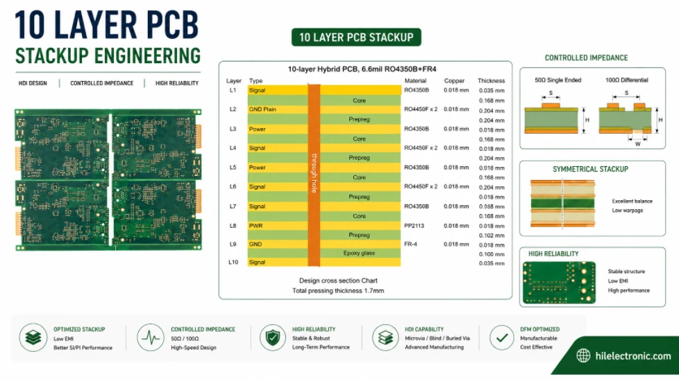
Figure 1. 10 layer PCB stackup for impedance and plane planning. Table of Contents Choose a Layer Architecture Before Choosing Dielectric Thickness Three Useful 10 Layer Stackup Archetypes A Reference-Plane-Rich 10 Layer Example Press-Out, Copper and Impedance Closure...

10 Layer PCB Routing Rules for DDR5, PCIe and Crosstalk

10 Layer PCB Routing Rules for DDR5, PCIe and Crosstalk

Figure 1. 10 layer PCB routing rules for DDR5 PCIe and crosstalk. Table of Contents Freeze the Electrical Rules Before Routing Begins Layer Assignment and Return-Path Continuity Differential Pairs: Geometry, Skew and Transitions DDR5 and Other Parallel Memory...

10 Layer PCB Manufacturer for Rigid, Flex and Rigid-Flex

10 Layer PCB Manufacturer for Rigid, Flex and Rigid-Flex

Figure 1. 10 layer PCB manufacturer production capability. Table of Contents 10 Layer PCB Manufacturer for Rigid, Flex and Rigid-Flex Boards How to Choose a 10 Layer PCB Manufacturer 10 Layer PCB DFM, Material Selection and Design Support Before Production 10 Layer...

13 Basic Rules of PCB Layout (and the Failures They Prevent)

13 Basic Rules of PCB Layout (and the Failures They Prevent)

Figure 1. 13 Basic Rules Of Pcb Layout reference image for PCB manufacturing review. Quick answer: Good PCB layout follows a short set of disciplines: plan the floorplan first, keep return paths tight over a solid ground plane, decouple power at each pin, separate...

How to Clean Flux Off a PCB: The Right Method for Each Flux Type

How to Clean Flux Off a PCB: The Right Method for Each Flux Type

Figure 1. How To Clean Flux Off Pcb reference image for PCB manufacturing review.Cleaning flux off a board sounds trivial until you use the wrong solvent on the wrong residue and end up with a hazy, corroded, or even more contaminated PCB. How to clean flux off a PCB...

PCB QR Code Size and Placement: Design Rules for Reliable Scanning

PCB QR Code Size and Placement: Design Rules for Reliable Scanning

Figure 1. PCB QR code size and placement image for PCB manufacturing review.PCB QR code size and placement determine whether scanners can read a board consistently through assembly, test, shipping, and field service. A code that is too small, too reflective, or too...