
10 Layer PCB Stackup Design for Impedance and Planes

Figure 1. 10 layer PCB stackup for impedance and plane planning.
Table of Contents
- Choose a Layer Architecture Before Choosing Dielectric Thickness
- Three Useful 10 Layer Stackup Archetypes
- A Reference-Plane-Rich 10 Layer Example
- Press-Out, Copper and Impedance Closure
- Power Integrity, Return Paths and EMI
- Symmetry, Copper Balance and Bow/Twist Risk
- Hybrid Materials, HDI and Rigid-Flex Variants
- Stackup Release Package and DFM Gate
- Common Stackup Errors and Their Consequences
- Reconcile the Finished Thickness Before Layout Release
- Heavy Copper, RF and Thermal Special Constructions
- Stackup Change Control After Layout Starts
- Stackup Sign-Off Checklist
A ten-layer stackup is an electrical and manufacturing architecture, not a list of copper layers separated by nominal prepreg thicknesses. It determines which signals have continuous references, how much routing capacity is available, where power is distributed, what trace geometry is manufacturable and how the panel behaves during lamination. Because ten copper layers create nine dielectric gaps, an apparently small change in one gap can alter impedance, total thickness and symmetry.
The examples below are design starting points rather than fabrication-release stackups. Final core and prepreg constructions, pressed thicknesses, copper foils and controlled geometries must be confirmed by the fabricator. Use this page with the material guide and impedance specification.
Choose a Layer Architecture Before Choosing Dielectric Thickness
Begin by classifying the design: number of high-speed routing channels, required power planes, BGA escape density, sensitive analog or RF sections, through-via or HDI structure, finished thickness and mechanical constraints. The goal is not to maximize layers labeled “signal.” The goal is to give each critical route a usable reference, keep return paths continuous and retain enough plane area for power distribution.
| Architecture question | Effect on the layer order |
|---|---|
| How many critical high-speed layers are needed? | Critical layers should be adjacent to continuous reference planes; the highest-speed stripline layers ideally sit between two reference planes. |
| How many power domains require broad copper? | Dedicated planes improve spreading inductance and current distribution, but split planes should not become accidental references for unrelated signals. |
| Is BGA escape through-hole or HDI? | Blind-via spans and sequential buildup can constrain which layers are practical for fanout and may change the lamination sequence. |
| Is the board thickness fixed? | Nine dielectric gaps and ten copper layers must fit the target while preserving manufacturable core/prepreg constructions. |
| Are low-loss or RF materials used selectively? | Material placement should be mechanically balanced and compatible with the bonding and drilling process. |
| Is the board rigid-flex? | Flex-layer continuity, coverlay, adhesive or adhesiveless construction and rigid-zone terminations must be defined before layer numbering is finalized. |
Routing direction is a secondary decision. Assigning “horizontal” and “vertical” layers does not repair a stackup with adjacent high-speed signal layers and no reference plane. Resolve field and return-path structure first, then allocate preferred directions based on placement and congestion.
Three Useful 10 Layer Stackup Archetypes
| Archetype | Typical layer-function ratio | Where it works well | Main trade-off |
|---|---|---|---|
| Reference-plane-rich | 4 signal / 4 ground / 2 power | High-speed serial, memory and mixed-signal boards where four routing layers are sufficient. | Less raw routing capacity; placement and BGA escape must be planned early. |
| Ground-reference-rich | 4 signal / 5 ground / 1 power, with additional power pours | Noise-sensitive designs with many signals referenced to ground and localized power distribution. | One dedicated power plane may be insufficient for wide current distribution. |
| Routing-density-focused | 6 signal / 3 ground / 1 power or another four-plane arrangement | Dense digital boards where two additional signal layers are necessary. | Some signal layers may face each other or reference split power, increasing crosstalk and return-path risk. |
The ratio alone does not prove a stackup is good. Two “6 signal / 4 plane” arrangements can behave very differently depending on where the planes are placed. If a design needs six signal layers, reserve the plane-adjacent layers for critical nets and place slower, shorter or orthogonally routed signals on the less favorable pair.
A Reference-Plane-Rich 10 Layer Example
The following layer order is a robust conceptual starting point for a rigid board with four principal signal layers. It is electrically symmetric in the critical signal environments and can be made mechanically symmetric by mirroring dielectric and copper constructions. It does not publish universal dielectric thicknesses or trace widths.
| Layer / gap | Function | Design intent |
|---|---|---|
| L1 | Signal and components | Short breakout and surface routing referenced to L2 ground. |
| L1-L2 | Thin prepreg selected by impedance and manufacturability | Keeps the surface return path close and supports practical trace width. |
| L2 | Continuous ground | Reference for L1 and one reference for L3. |
| L2-L3 | Core or prepreg | One side of the L3 stripline environment. |
| L3 | High-speed signal | Stripline between L2 and L4 grounds. |
| L3-L4 | Core or prepreg | Mirrored or intentionally controlled with L2-L3. |
| L4 | Continuous ground | Second L3 reference and ground partner for L5 power. |
| L4-L5 | Relatively thin dielectric where power-plane capacitance is useful | Pairs the first power plane with ground; final thickness follows voltage, capacitance and fabrication needs. |
| L5 | Primary power | Broad, defined power domains; do not use fragmented areas as uncontrolled signal references. |
| L5-L6 | Central core or bonding region | Can absorb thickness; this power-to-power gap is not claimed as a ground-referenced decoupling pair. |
| L6 | Secondary power | Second broad power domain, paired outward with L7 ground. |
| L6-L7 | Relatively thin dielectric | Power-ground pair for the lower half of the stack. |
| L7 | Continuous ground | Reference for L8 and ground partner for L6. |
| L7-L8 | Core or prepreg | One side of the L8 stripline environment. |
| L8 | High-speed signal | Stripline between L7 and L9 grounds. |
| L8-L9 | Core or prepreg | Completes the lower stripline and mirrors the upper signal region. |
| L9 | Continuous ground | Reference for L10 and one reference for L8. |
| L9-L10 | Thin prepreg selected by impedance and manufacturability | Mirrors the L1-L2 surface environment. |
| L10 | Signal and components | Bottom-side breakout and surface routing referenced to L9. |
This arrangement gives both inner signal layers two ground references and keeps each outer signal next to ground. Each central power plane has an outward ground partner. The central L5-L6 spacing can be selected for total thickness and mechanical balance without being misrepresented as a power-ground decoupling pair.
Designs needing more routing can convert a plane to signal, but the consequences must be explicit. For example, converting L6 to signal removes a broad power plane and creates a signal layer adjacent to L5 power and L7 ground. Critical routes on that layer must avoid L5 splits or be designed to reference L7 predominantly.
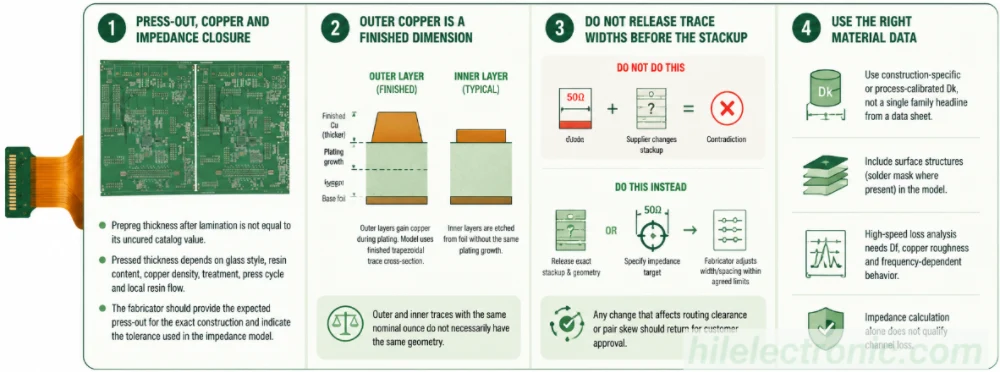
Press-Out, Copper and Impedance Closure
Prepreg thickness after lamination is not equal to its uncured catalog value. Pressed thickness depends on glass style, resin content, copper density, treatment, press cycle and local resin flow. The fabricator should provide the expected press-out for the exact construction and indicate the tolerance used in the impedance model.
Outer copper is a finished dimension
Outer layers begin with base foil and gain copper during hole and pattern plating. The controlled-impedance model should use the finished trace cross-section, including trapezoidal etch shape. Inner layers are usually etched from foil without the same pattern-plating growth, so an outer and inner trace with the same nominal ounce designation do not necessarily share the same geometry.
Do not release trace widths before the stackup
A drawing that fixes 50 Ω at a particular width while allowing the supplier to change dielectric construction creates a contradiction. Either release the exact stackup and geometry, or specify the impedance target and authorize the fabricator to adjust width/spacing within agreed limits. Any change that affects routing clearance or pair skew should return for customer approval.
Use the right material data
The field solver should use construction-specific or process-calibrated Dk, not a single family headline copied from a data sheet. Surface structures should include solder mask where present. High-speed loss analysis additionally needs Df, copper roughness and frequency-dependent behavior; the impedance calculation alone does not qualify channel loss.
Power Integrity, Return Paths and EMI
Closer signal-to-reference spacing reduces loop inductance and field spread, but the exact improvement is geometry-dependent; it should not be advertised as a fixed dB reduction. Plane pairs can provide distributed capacitance, yet their value follows the parallel-plate relationship and actual overlap area. A thin power-ground dielectric can be useful, but it does not eliminate discrete decoupling or package inductance.
Keep high-speed reference planes continuous. When a power plane contains multiple islands, do not place critical routes where the dominant return current would have to cross an island boundary. If a signal layer is between power and ground, decide which plane is the intended reference and ensure the alternative path is controlled.
Edge via fences can help selected RF or enclosure-current problems, but a universal fixed pitch around every digital board is unnecessary and may reduce routing or create plane perforation. Fence pitch and termination should follow the highest frequency and enclosure strategy being controlled.
Plan the return path at every layer transition
A signal via changes the electromagnetic field from one transmission-line structure to another. When both routing layers reference ground planes, nearby ground vias can connect those planes and reduce the return-path loop, but their number and placement should follow the transition geometry rather than a universal distance rule. When a route changes between layers referenced to different conductors, such as ground on one layer and a power plane on another, the return current needs a deliberate transfer path. That path may use a suitably placed decoupling capacitor between the reference conductors, a different layer assignment, or a redesigned transition that keeps both segments referenced to ground.
The stackup drawing should therefore identify the intended reference for each controlled layer, not merely label a layer as “signal.” Via fields, anti-pads and plane clearances must be reviewed together because an electrically sound layer order can still be undermined by a transition that removes too much nearby reference copper.
Symmetry, Copper Balance and Bow/Twist Risk
Mechanical symmetry means more than assigning the same net names across the centerline. Pair the outer copper weights, dielectric constructions and expected copper coverage. A high-density component side can have much more copper than the opposite side even when nominal foil weights match; CAM thieving or design balancing may be needed.
Bow and twist acceptance is governed by the applicable product specification and assembly need. Fine-pitch BGA assembly may require tighter flatness than a generic bare-board limit. The stackup review should therefore consider panel size, board outline, copper distribution, cutouts, material mix and depanelization method, not only layer symmetry.
| Balance check | Evidence before release |
|---|---|
| Copper weight | Mirrored base/finished copper or a documented asymmetric process approved by the fabricator. |
| Dielectric construction | Paired core/prepreg types and press-out where mechanical balance is intended. |
| Copper area | Layer plots or CAM analysis identifying large imbalance and proposed thieving. |
| Material placement | Low-loss, RF or flex materials distributed with a qualified lamination plan. |
| Panel and outline | Expected array, rails, breakaways, slots and large cutouts included in warpage review. |

Figure 2. 10 layer PCB stackup layer arrangement example.
Hybrid Materials, HDI and Rigid-Flex Variants
Hybrid low-loss construction
Low-loss material can be localized around selected signal layers, but the exact core, prepreg or bondply arrangement must be qualified. Do not impose a universal CTE-difference threshold and assume compatibility. Review resin flow, adhesion, cure, dimensional movement, drill/desmear process and plated-hole reliability for the complete material pair.
HDI buildup
In a 1+8+1, 2+6+2 or 3+4+3 board, the layer notation describes buildup distribution, not the full manufacturing route by itself. Each buildup level adds imaging, lamination, laser drilling, metallization and, where required, filling/planarization. The stackup must identify every microvia span, buried via, through via and the order in which structures are formed. Press-cycle counting should include the central subcomposite and each sequential buildup, using the supplier’s defined terminology.
Rigid-flex stackup
A ten-layer rigid-flex board does not necessarily carry all ten layers through the bend zone. Often only selected flex layers continue while other copper layers terminate in the rigid region. The design should identify flex-layer count, adhesiveless or adhesive construction, coverlay, stiffeners, copper type, bend direction and static or dynamic duty. IPC-2223 is a design standard; finished flexible and rigid-flex board performance is addressed by IPC-6013.
Stackup Release Package and DFM Gate
A production stackup should be revision-controlled and include all ten copper layers, all nine dielectric gaps, material grade and construction, core/prepreg designation, nominal and tolerance thickness, copper type and thickness, finished board thickness, controlled structures, via spans and any sequential-lamination notes.
| Release item | Acceptance question |
|---|---|
| Layer function | Are reference planes continuous where critical routes require them? |
| Material construction | Are exact grades, glass styles or approved substitution rules identified? |
| Copper definition | Are base and finished outer copper distinguished? |
| Press-out | Are dielectric values production estimates rather than uncured catalog values? |
| Impedance geometry | Does each controlled class point to the correct layer and reference? |
| Via architecture | Are through, blind, buried, microvia and back-drill spans unambiguous? |
| Mechanical balance | Has copper area, panelization and mixed-material placement been reviewed? |
| Approval authority | Is it clear which stackup or artwork changes require customer sign-off? |
Complete this gate before routing sign-off. A “final stackup after Gerber submission” workflow forces avoidable artwork changes and can invalidate timing and channel simulation. Submit the construction through the DFM review with the controlled-impedance table and critical routing assumptions.
Common Stackup Errors and Their Consequences
Counting functions incorrectly
A layer table that claims six signal layers but lists only four signal layers undermines the entire design rationale. Count copper functions directly and verify every signal’s reference environment.
Omitting dielectric gaps
Ten copper layers require nine dielectric separations. A table that lists dielectric only “below” selected layers often omits or double-counts gaps and cannot reconcile to finished thickness.
Using universal trace widths
Fixed 50 Ω or 100 Ω dimensions copied from another construction should not appear as fabrication-ready rules. They must be recalculated with the actual pressed dielectric, copper and material model.
Calling two power planes a decoupling pair
Distributed plane capacitance is useful between conductors carrying opposite charge, typically power and ground. Two adjacent power planes on different rails are not a general replacement for a power-ground pair and may introduce coupling between rails.
Assuming electrical labels create mechanical symmetry
Warpage depends on material, thickness and copper distribution. Mirrored layer names are not enough if one side has dense copper and the other has sparse routing.
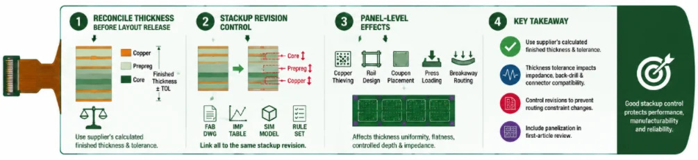
Reconcile the Finished Thickness Before Layout Release
The nominal board thickness is the result of all nine pressed dielectric gaps, ten copper layers, plating contribution and the supplier’s measurement convention. A simple sum of catalog cores and prepregs can be wrong because copper becomes embedded in resin and outer plating is added after lamination. The released stackup should show the supplier’s calculated finished value and tolerance, then confirm that connector, press-fit, card-edge and enclosure requirements use the same definition.
Thickness tolerance also changes impedance and back-drill geometry. A design near the limit of a connector’s contact range or a controlled-depth drill window may require tighter construction control than an ordinary board. If a thinner board is proposed to reduce via length, check stiffness, assembly handling, warpage and connector compatibility rather than treating thickness only as an electrical variable.
Stackup revision control
Give every approved stackup a revision and link the fabrication drawing, impedance table, simulation model and layout rule set to that revision. A supplier-proposed change in core, prepreg, copper or material should generate a redlined stackup and identify which controlled geometries change. This prevents an apparently minor purchasing substitution from silently invalidating routing constraints.
Panel-level effects
The same board outline can behave differently when arrayed on a different production panel. Copper thieving, rail design, coupon placement, press loading and routing of breakaway features can influence thickness uniformity and bow/twist. Include panelization in the first-article review when flatness, controlled depth or impedance sampling is critical.
Heavy Copper, RF and Thermal Special Constructions
Heavy copper changes more than current capacity. Thick foil requires greater etch allowance, affects minimum trace and space, increases resin demand during lamination and can make copper balance more difficult. A ten-layer board with selected heavy-power layers may need resin-filled prepreg constructions, stepped copper or localized bus structures rather than uniformly heavy copper on every layer. The supplier should provide achievable geometry for the exact copper thickness and panel size.
RF layers can be placed on the outside or within a hybrid stackup depending on launch access, shielding and material processing. Controlled RF structures may require coplanar ground, via fences, cavity or edge plating and a nickel-free finish in selected applications. These features should be treated as a specific distributed-circuit design; IPC-2228 and the selected material supplier’s process guidance may be relevant. They should not be reduced to “use Rogers on L1.”
Embedded copper coins, thermal inlays and metal heat spreaders create local thickness, plating and lamination constraints. Their interfaces, isolation, planarity and thermal path must be defined before the stackup is released. A thermal feature can disturb nearby impedance or warpage if it is added after routing. Coordinate the thermal model, mechanical drawing and electrical layer order as one design.
For any special construction, request a cross-section drawing and process-specific DFM response. The general ten-layer capability table should not imply that every heavy-copper, RF, flex and embedded-thermal option can be combined without a project qualification.
Stackup Change Control After Layout Starts
Once routing rules, delay targets and channel models have been tied to an approved stackup, a material or construction change is an engineering change rather than a purchasing substitution. Changes to core or prepreg construction, resin content, copper foil, finished copper, solder mask, via span or lamination sequence can affect more than one design constraint at the same time.
| Proposed change | Checks that should be repeated | Required release evidence |
|---|---|---|
| Core, prepreg, resin content or material grade | Pressed thickness, impedance, propagation delay, loss, total thickness and lamination compatibility | Redlined stackup and updated controlled-geometry calculation |
| Copper foil type, profile or finished thickness | Etch capability, trace cross-section, impedance, conductor loss, current capacity and copper balance | Updated artwork assumptions and, where relevant, revised loss model |
| Via span, back-drill depth or HDI buildup | Pad stack, antipad, registration, lamination sequence, stub resonance and reliability qualification | Revised drill drawing, cross-section and qualification plan |
| Panelization, rail design or coupon placement | Bow/twist, copper distribution, press loading, coupon correlation and controlled-depth features | Approved panel drawing or first-article review record |
When procurement needs an alternate dielectric thickness, rerun both the electrical and mechanical checks. Changing one prepreg can alter trace width, pair spacing, propagation delay, total thickness and resin balance. The revised drawing should identify the new construction rather than preserving the old revision number. This discipline is especially important when a stackup is reused across several products or manufacturing sites.
Stackup Sign-Off Checklist
A stackup is ready for layout release when the electrical architecture and the manufacturable material construction have been reconciled. The sign-off package should show all ten copper layers and all nine dielectric gaps, identify the reference plane for every controlled signal layer, and close the finished-thickness calculation using pressed-not catalog-dielectric values.
- Confirm layer functions, reference continuity and power-plane segmentation.
- Balance dielectric construction, copper distribution and special materials about the mechanical center where practical.
- Identify the exact core, prepreg, resin-content and copper-foil options used in the impedance and loss models.
- Resolve HDI sublaminations, buried vias, flex transitions and hybrid-material bonds before final numbering.
- Return production widths, pair gaps and finished thickness for approval.
- Lock the stackup revision before routing constraints and delay-matching rules are finalized.
A useful stackup drawing is both an electrical model boundary and a manufacturing instruction. If it cannot explain the return path, total thickness, copper construction and lamination sequence, it is not ready for release.

Recommended Posts

Taconic RF-35 PCB Manufacturing Service — Prototype Through Volume Production
Figure 1. Taconic RF-35 PCBTaconic RF-35 is the workhorse...

Isola Astra MT77 PCB Manufacturing
Figure 1. Isola Astra MT77 PCB ManufacturingIsola Astra...

Custom Rogers RO4835 PCB Fabrication & Assembly Services
Figure 1. Rogers RO4835 PCBRogers RO4835 PCB is a...

Nelco N4000-13 PCB Material and Manufacturing Guide | Highleap Electronics
Figure 1. Nelco N4000-13 PCBNelco N4000-13 PCB is a...
How to get a quote for PCBs
Let’s run DFM/DFA analysis for you and get back to you with a report. You can upload your files securely through our website. We require the following information in order to give you a quote:
-
- Gerber, ODB++, or .pcb, spec.
- BOM list if you require assembly
- Quantity
- Turn time
For PCBA services, please provide your BOM (Bill of Materials) and any specific assembly instructions. We also offer DFM/DFA analysis to optimize your designs for manufacturability and assembly, ensuring a smooth production process.