
10 Layer PCB Materials for FR-4, Low-Loss and RF Boards
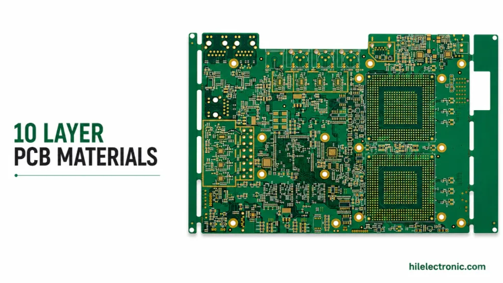
Figure 1. 10 layer PCB materials for FR-4 low-loss and RF boards.
Table of Contents
- Start with the Electrical and Reliability Requirement
- How to Read a Laminate Data Sheet Without Mixing Test Methods
- Material Families Used in 10 Layer Boards
- Copper Foil, Glass Weave and Resin Content
- Hybrid Material Stackups and Substitution Control
- Thermal Reliability, HDI and Assembly Exposure
- What to Put on the Fabrication Drawing and Purchase Order
- Material Cost Without Misleading Percentage Adders
- Availability, Regulatory Status and Long-Term Supply
- Material Selection Sign-Off
- Material Qualification Dossier for Repeat Production
Material selection for a 10 layer PCB is not a lookup table that converts an interface name into a laminate brand. A board carrying DDR5, PCI Express or a high-speed SerDes may be manufacturable on several resin systems, depending on channel length, copper profile, trace geometry, connector loss, via transitions, temperature exposure and the receiver’s equalization capability. Conversely, a short route can fail on an expensive laminate if the return path, via field or reference-plane transition is poor.
This guide treats material choice as an engineering decision rather than a marketing hierarchy. It explains what the published properties mean, where data-sheet numbers can be compared, how copper and glass affect the finished channel, and what must be controlled when two materials are combined in one stackup. Project-specific choices should be reviewed together with the 10 layer stackup and the high-speed channel plan before layout is frozen.
Start with the Electrical and Reliability Requirement
A useful material decision begins with the conditions the finished board must survive and the electrical performance the routed channel must deliver. The minimum input set is the signaling spectrum or compliance mask, maximum routed length, allowed insertion loss, expected number and type of via transitions, reference-plane arrangement, assembly profile, product temperature range and required reliability class. Material is then selected as one part of the total loss and reliability budget.
| Question | Why it matters | Evidence to request |
|---|---|---|
| What frequency range must be modeled? | Dk and Df are frequency- and method-dependent. The relevant range is set by edge spectrum and modulation, not only the headline bit rate. | Construction-specific Dk/Df data, test method, frequency and copper profile. |
| How much board loss is available? | Package, connector, via and trace losses share one channel budget. A laminate cannot be selected from trace length alone. | A channel budget or simulation showing the allocation to the PCB. |
| How many thermal excursions occur? | Sequential lamination, via filling, surface finish, assembly reflow and rework all add heat exposure. | Assembly profile, HDI buildup, T260/T288 or equivalent thermal data, Z-axis expansion and qualification results. |
| Is the board rigid, flex or rigid-flex? | Flex regions require a material and copper system chosen for bend behavior, not merely low Df. | Flex-layer count, bend radius, static or dynamic duty, copper type and coverlay construction. |
| May the fabricator substitute a grade? | Two products in the same loss category can have different Dk, resin flow, cure behavior, copper adhesion and available glass styles. | Approved-material list and a written requalification path for substitutions. |
“High Tg,” “low loss” and “RF material” are categories, not complete specifications. The selected grade, resin content, glass style, core thickness, prepreg construction and copper foil must all be identified before final impedance geometry or channel simulation is considered released.
How to Read a Laminate Data Sheet Without Mixing Test Methods
Published values are often measured by different methods. A clamped stripline value, a resonator value and an impedance-derived design value are not interchangeable even when they are reported at the same frequency. The data may also describe a nominal resin system rather than the exact glass-and-resin construction used in the stackup. For this reason, a single Dk number copied into a field solver can produce a plausible but inaccurate trace width.
| Property | What it tells the designer | Common interpretation error |
|---|---|---|
| Dk or dielectric constant | Controls phase velocity and contributes to impedance. The effective value seen by a trace also depends on field distribution, resin content and glass. | Comparing values measured by different methods as if they were directly equivalent. |
| Df or dissipation factor | Describes dielectric loss under the stated method and frequency. It is only one part of insertion loss. | Turning a headline Df into a universal dB-per-inch number without geometry and copper data. |
| Tg | Marks a transition in mechanical behavior of the cured resin system. | Assuming higher Tg alone guarantees better plated-hole or reflow reliability. |
| Td, T260 and T288 | Describe decomposition or time-to-delamination behavior under stated tests. | Using Td by itself to decide whether a material is suitable for sequential lamination. |
| Z-axis CTE | Helps estimate strain imposed on plated holes as the dielectric expands through thickness. | Ignoring the above-Tg region and the total thermal history of the product. |
| Moisture absorption and CAF resistance | Affect electrical stability and electrochemical reliability in humid service. | Treating a low headline moisture value as a substitute for product-level qualification. |
| Peel strength | Indicates copper-to-dielectric adhesion under the specified foil and treatment. | Assuming the value remains unchanged after alternative oxide, low-profile copper or repeated heat exposure. |
For impedance, the fabricator normally uses a process-calibrated “design Dk” or an empirical model associated with a particular material construction. For insertion-loss simulation, the model should additionally identify copper roughness and, at higher frequencies, the actual glass style or an equivalent anisotropic representation. The model used for design and the material delivered by purchasing must refer to the same construction.
Material Families Used in 10 Layer Boards
Conventional and high-temperature FR-4 systems
FR-4 covers a broad family of woven-glass reinforced thermoset laminates. It is suitable for many industrial, control, power and moderate-speed digital boards, but the exact grade still matters. A ten-layer board with multiple reflow cycles, high aspect-ratio plated holes or sequential lamination may need lower Z-axis expansion, longer delamination time and better CAF performance than a simple two-layer product. “RoHS compliant” does not automatically mean that every FR-4 grade is appropriate for every lead-free assembly profile.
High-Tg FR-4 is often selected for thermal and dimensional margin, not because Tg directly determines signal speed. A short, well-routed high-speed channel may work on a good FR-4 system; a longer channel may require lower dielectric and conductor loss. The decision should come from loss analysis and reliability needs rather than a protocol-to-material slogan.
Low-loss digital laminates
Families such as Panasonic MEGTRON, Isola I-Tera and comparable high-speed systems reduce dielectric loss and are commonly offered with smoother copper options. They are not automatically interchangeable. Each family contains multiple grades, and the exact Dk/Df values depend on product variant, test method, resin content and glass construction. For example, current I-Tera MT40 literature presents headline values around Dk 3.45 and Df 0.0031, while the construction tables show that individual cores and prepregs vary. That construction-level variation is exactly why an approved stackup must identify more than the family name.
MEGTRON 6, MEGTRON 7 and MEGTRON 8 represent different product families and performance levels. A designer should specify the required electrical and process characteristics or a precise grade-not write “M6 or equivalent” and allow an uncontrolled replacement. At the highest data rates, the copper option and via architecture can dominate the difference between two nominally low-loss dielectrics.
Ultra-low-loss and very-high-speed systems
Isola Tachyon 100G is an example of an ultra-low-loss system. Its current product sheet lists headline values near Dk 3.02 and Df 0.0021, but its detailed construction tables again show variation by glass and resin content. These materials are chosen when the channel analysis justifies them; they should not be described as a mandatory default for every 112G or PCIe design.
Hydrocarbon/ceramic and PTFE-based RF laminates
a specialty low-loss laminate and a specialty low-loss laminate are woven-glass reinforced hydrocarbon/ceramic thermoset laminates, not PTFE laminates. a specialty low-loss laminate is published around Dk 3.38 and Df 0.0027 at 10 GHz; a specialty low-loss laminate provides a related process-compatible option with different electrical and flammability characteristics. specialty low-loss laminate also supplies true PTFE-based families such as selected a PTFE-based low-loss laminate a specialty low-loss laminate products. The correct family depends on frequency, loss, Dk tolerance, thermal expansion, plated-through-hole requirements, flammability and fabrication process.
Mixing an RF core into an otherwise FR-4 multilayer can be effective, but the bonding material, copper treatment, drilling and surface finish must be selected for the complete construction. A brand name alone does not define a manufacturable hybrid.
Polyimide systems for flex and rigid-flex
Flexible circuits use polyimide films, adhesive systems or adhesiveless copper-clad laminates, coverlay and selected copper foils. DuPont Pyralux AP is an adhesiveless flexible laminate family; Pyralux TK is aimed at lower-loss flexible applications. The appropriate choice depends on bend duty, layer count, impedance, temperature and the rigid-flex lamination process. Static installation bends and continuous dynamic flexing are different design problems and should not share one generic bend-radius claim.
Copper Foil, Glass Weave and Resin Content
Copper roughness belongs in the loss model
At high frequency, current crowds toward the conductor surface. A rough bonding surface lengthens the effective current path and increases conductor loss. Standard electrodeposited foil, reverse-treated foil, very-low-profile and hyper-very-low-profile products can therefore produce different insertion loss on the same dielectric. The trade-off is not simply “smoother is better”: adhesion, oxide treatment, resin chemistry, handling and cost must remain compatible with the fabrication process.
The fabrication drawing should identify either the approved foil class or the maximum roughness model used in simulation. Marketing labels such as VLP and HVLP are not perfectly standardized across suppliers, so a project may need a supplier-specific foil designation or a measurable roughness requirement.
Glass weave changes local Dk and skew
Woven glass and resin have different dielectric properties. A narrow trace or one member of a differential pair can travel predominantly over glass bundles while the adjacent trace travels over resin-rich regions, creating local delay mismatch. Spread-glass constructions, diagonal routing relative to the weave, wider traces, larger pair spacing where appropriate, and randomized artwork orientation are mitigation options. The right choice depends on the actual glass style and the skew budget.
Resin content also affects pressed thickness and effective Dk. Prepreg is not a fixed-thickness plastic sheet: its final thickness depends on glass style, resin content, copper density, press cycle and local resin flow. Stackup calculations should therefore use the fabricator’s press-out model rather than nominal catalog thickness alone.
Hybrid Material Stackups and Substitution Control
A hybrid stackup places a low-loss or RF material only where it creates measurable value, such as around selected stripline channels or an RF surface layer. This can reduce material consumption, but it adds engineering work. The fabricator must qualify the bondply or prepreg, cure cycle, resin flow, inner-layer treatment, dimensional compensation, drilling, desmear and plated-hole reliability for the combined system.
| Control item | Why it must be agreed before release |
|---|---|
| Exact material and construction | The same family can contain multiple resin systems, glass styles and copper options. |
| Approved bonding layer | Adhesion and flow must suit both materials and the local copper density. |
| Press cycle and dimensional compensation | Different materials move differently through heat and pressure; artwork scaling may be construction-specific. |
| Hole preparation | PTFE, hydrocarbon/ceramic, filled resin and conventional epoxy systems can require different treatment. |
| Impedance recalculation | A substitution changes Dk, pressed thickness and often copper profile. |
| Reliability evidence | The mixed system should be represented by coupons or prior qualification relevant to the via and thermal exposure. |
Material substitution should be handled in one of three ways: no substitution without written approval; substitution only from a named approved list; or controlled substitution after the supplier provides a revised stackup, impedance calculation and required qualification evidence. “Equivalent performance class” is not sufficient authorization.
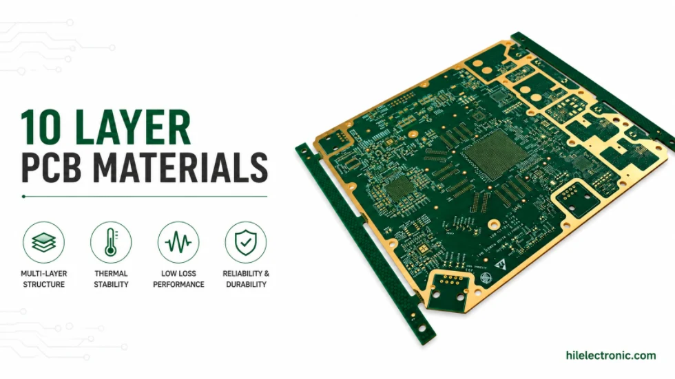
Figure 2. 10 layer PCB material selection and laminate stackup.
Thermal Reliability, HDI and Assembly Exposure
Ten-layer reliability is influenced by total thermal history. A conventional multilayer may see one primary lamination cycle, while an HDI construction adds sequential buildup cycles and may include copper filling, planarization and additional curing operations. Surface finish, component assembly and rework then add more exposure. The material system must tolerate the entire route, not just one reflow peak.
Relevant evidence can include T260/T288 behavior, Z-axis CTE, moisture conditioning, reflow simulation, thermal stress microsections and interconnect testing. The applicable tests and sample frequency should be defined by the product specification and risk. It is inaccurate to claim that a particular Td value automatically makes a material “required” for a given number of buildup layers. Via geometry, resin system, copper plating, moisture, press cycle and coupon design all contribute.
For HDI, the dielectric thickness under a microvia is selected together with the laser diameter and capture land. Repeated stacked microvias require a process with demonstrated filling and interfacial reliability. The material page should support that decision, while the actual buildup and acceptance plan belong in the 10 layer HDI engineering specification.
What to Put on the Fabrication Drawing and Purchase Order
A purchase order that says only “high-Tg FR-4” or “MEGTRON equivalent” leaves too much open. A production-ready material note should identify the approved grade or performance specification, the substitution rule, copper foil requirements, flammability or regulatory needs, material traceability level and any construction-specific electrical data used by the design.
| Required entry | Example of a useful instruction |
|---|---|
| Material approval | Use the named grade and construction, or obtain written approval before substitution. |
| Electrical model | Use the fabricator-approved design Dk for impedance; provide construction-specific Dk/Df and foil model for channel simulation. |
| Copper foil | Identify approved supplier/foil class or the roughness envelope assumed in simulation. |
| Glass style | Identify required spread-glass or prohibited constructions where skew is critical. |
| Traceability | State whether certificates of conformance, lot identity or laminate certificates are required. |
| Thermal qualification | State the assembly profile and any required coupon, reflow simulation or interconnect test. |
| Hybrid approval | Require a released stackup and lamination process for the exact material pair. |
Submit these notes together with the impedance table and stackup. The controlled-impedance guide explains what the fabricator needs to calculate and verify the final geometry.
Material Cost Without Misleading Percentage Adders
Material cost is influenced by sheet price, minimum purchase quantity, usable panel size, shelf life, required copper option, prepreg availability and the yield of the complete stackup. A hybrid construction can reduce expensive dielectric area, but it may add procurement, layup and qualification complexity. Conversely, a full low-loss build can sometimes simplify purchasing and lamination even though the raw material is more expensive.
For budgeting, ask the supplier to separate the effect of the material system from HDI cycles, finish, testing and documentation. Do not treat a fixed percentage found on a web page as a quotation. The 10 layer PCB cost guide provides a cost-driver model that can be used to compare alternatives without inventing universal price multipliers.
Request a Material and Stackup Review
Availability, Regulatory Status and Long-Term Supply
Material availability is a design constraint when a board will remain in production for years. A grade may be technically suitable but available only in selected thicknesses, copper foils or panel sizes. Minimum purchase quantities, shelf-life controls and regional stocking can dominate prototype lead time. Before freezing a niche construction, confirm that the required core and prepreg combinations are part of the manufacturer’s current offering and that the fabricator has an approved process for them.
Flammability, halogen-free claims, RoHS/REACH declarations and UL recognition are separate questions. A laminate may be RoHS compatible but not meet the flame rating required by the end product; a particular construction may fall outside the thickness range of a recognition. The purchase specification should identify the required regulatory evidence and the manufacturing site to which it applies. Do not infer certification from a family name or from another factory’s qualification.
For long-life programs, maintain a controlled approved-material list with at least one technically reviewed alternate where practical. The alternate should be evaluated before a supply interruption, not introduced during a shortage without impedance, lamination and reliability review. Last-time-buy, change-notification and requalification responsibilities should be included in the supplier agreement.
Material Selection Sign-Off
A material decision is ready for release when purchasing language, stackup construction and electrical models refer to the same grade and construction. Generic descriptions such as “high Tg,” “low loss” or “equivalent” are insufficient when impedance, insertion loss or repeated thermal exposure matters.
- State the approved grade or approved-material list and the written substitution process.
- Identify core and prepreg constructions, resin content, glass style and copper profile used by the models.
- Record the Dk/Df test method, frequency and whether the value is a laminate data-sheet value or a design model.
- Check thermal history from sequential lamination, via filling, finish, assembly reflow and expected rework.
- Confirm availability, minimum purchase quantity, lead-time risk, regulatory status and long-term supply needs.
- Require a revised stackup and impedance calculation whenever an approved substitution changes construction.
The best material is the least costly qualified system that satisfies the complete electrical, mechanical, thermal and supply requirement. A premium resin system cannot compensate for a poor return path, resonant via stub or uncontrolled substitution.
Material Qualification Dossier for Repeat Production
Programs that depend on electrical loss, repeated thermal exposure or long service life should retain a material dossier rather than only a supplier trade name. The dossier makes repeat orders, alternate-source reviews and failure analysis more reliable.
- manufacturer, exact grade, revision and regulatory status;
- approved core/prepreg constructions and available glass styles;
- copper foil type and treatment used on each controlled signal layer;
- Dk/Df data source, test method, frequency and design-model assumptions;
- thermal data relevant to the actual process sequence, including lamination and assembly exposure;
- process qualification or first-article evidence for plated holes, microvias and hybrid bonds;
- storage, shelf-life, bake and moisture-handling instructions where applicable;
- approved alternates and the conditions that trigger electrical or reliability requalification.
Material aging and availability also matter. A laminate can remain technically suitable while becoming commercially impractical because a core thickness, glass style or copper option is discontinued. Periodic lifecycle review should therefore occur before the last approved construction becomes unavailable. When a new revision of a material family is introduced, compare processing and construction data instead of assuming the trade name guarantees interchangeability.
For hybrid builds, retain the bond-ply, oxide or alternative treatment and lamination assumptions together with the signal-layer material. The dielectric carrying the signal may receive most attention, but the interface between material systems often controls dimensional behavior and long-term reliability.

Recommended Posts

TMM4 Filter PCB Manufacturing
TMM4 filter PCB manufacturing is controlled by the...

TMM3 PCB Manufacturing for RF Modules
TMM3 PCB manufacturing is most useful where the RF module...

TMM6 PCB Fabrication
TMM6 fabrication is the process-control page for a mid-Dk...

TMM10 PCB Manufacturing for Compact RF Designs
Table of contentsHow TMM10 Shrinks RF StructuresTMM10 vs...
How to get a quote for PCBs
Let’s run DFM/DFA analysis for you and get back to you with a report. You can upload your files securely through our website. We require the following information in order to give you a quote:
-
- Gerber, ODB++, or .pcb, spec.
- BOM list if you require assembly
- Quantity
- Turn time
For PCBA services, please provide your BOM (Bill of Materials) and any specific assembly instructions. We also offer DFM/DFA analysis to optimize your designs for manufacturability and assembly, ensuring a smooth production process.