Select Page

Your PCB Manufacturing Expert – Highleap Electronic

Laser Drilled PCB Vias Design Optimization and Costs

Laser Drilled PCB Vias Design Optimization and Costs

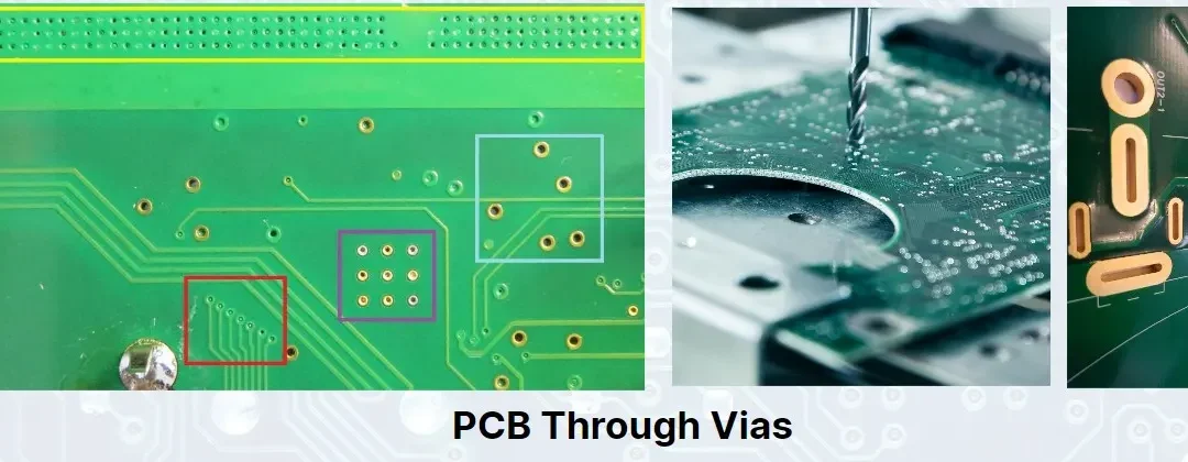
Figure 1. Laser drilling PCB Table of Contents When Does Your PCB Design Actually Need Laser Drilling? Microvia Design Rules: The Exact Numbers That Control Cost and Yield Aspect Ratio: The Single Most Expensive Mistake in HDI Design Via-in-Pad Rules and the Assembly...

In-Depth Guide to Via-Filling Plating in PCB Manufacturing

In-Depth Guide to Via-Filling Plating in PCB Manufacturing

The printed circuit board (PCB) industry, particularly electroplated PCB manufacturing, plays a pivotal role in the electronic components sector. This segment contributes a significant share to the overall global market, with a valuation approaching $60 billion...

Effective Impedance Control in mmWave PCBs with PTH Vias

Effective Impedance Control in mmWave PCBs with PTH Vias

Plated through-hole vias (PTH vias) are fundamental elements in printed circuit boards (PCBs), providing electrical connections between different layers. However, when working with mmWave frequencies (typically above 30 GHz), the design of these vias becomes more...

Highleap Electronic’s Guide to Blind and Buried Vias in PCBs

Highleap Electronic’s Guide to Blind and Buried Vias in PCBs

In the ever-evolving landscape of electronics, printed circuit boards (PCBs) serve as the backbone of virtually all electronic devices. As technology advances, the demand for more compact, high-performance, and reliable PCBs has surged. Central to meeting these...

PCB Side Plating Solutions for High-Performance Electronics

PCB Side Plating Solutions for High-Performance Electronics

[pac_divi_table_of_contents included_headings="off|on|off|off|off|off" exclude_headings_by_class="on" active_link_highlight="on" level_markers_2="icons" level_markers_3="icons" title_container_padding="10px|15px|10px|15px|true|false" title_container_bg_color="#EEEEEE"...

Metallized Half-Hole PCB Manufacturing Solutions

Metallized Half-Hole PCB Manufacturing Solutions

[pac_divi_table_of_contents included_headings="off|on|off|off|off|off" exclude_headings_by_class="on" active_link_highlight="on" level_markers_2="icons" level_markers_3="icons" title_container_padding="10px|15px|10px|15px|true|false" title_container_bg_color="#EEEEEE"...

Understanding PCB Non-Plated Through Holes (NPTH)

Understanding PCB Non-Plated Through Holes (NPTH)

[pac_divi_table_of_contents included_headings="off|on|off|off|off|off" exclude_headings_by_class="on" active_link_highlight="on" level_markers_2="icons" level_markers_3="icons" title_container_padding="10px|15px|10px|15px|true|false" title_container_bg_color="#EEEEEE"...

Common Problems with PCB Through Vias and Their Solutions

Common Problems with PCB Through Vias and Their Solutions

[pac_divi_table_of_contents included_headings="off|on|off|off|off|off" exclude_headings_by_class="on" active_link_highlight="on" level_markers_2="icons" level_markers_3="icons" title_container_padding="10px|15px|10px|15px|true|false" title_container_bg_color="#EEEEEE"...

Cost-Saving Back Drilling Technology for Multi-Layer PCBs

Cost-Saving Back Drilling Technology for Multi-Layer PCBs

[pac_divi_table_of_contents included_headings="off|on|off|off|off|off" exclude_headings_by_class="on" active_link_highlight="on" level_markers_2="icons" level_markers_3="icons" title_container_padding="10px|15px|10px|15px|true|false" title_container_bg_color="#EEEEEE"...

Guide to Micro Vias: Technology and Best Practices

Guide to Micro Vias: Technology and Best Practices

[pac_divi_table_of_contents included_headings="off|on|off|off|off|off" exclude_headings_by_class="on" active_link_highlight="on" level_markers_2="icons" level_markers_3="icons" title_container_padding="10px|15px|10px|15px|true|false" title_container_bg_color="#EEEEEE"...