
Cost-Saving Back Drilling Technology for Multi-Layer PCBs

Back drilling is an essential process in PCB manufacturing that removes unwanted via stubs, which can cause signal interference, degradation, and loss in high-frequency and high-speed applications. This article delves deeply into the technology, techniques, and best practices of back drilling, exploring when to consider this process, its advantages, and the technical steps involved in implementing it effectively.
What is Back Drilling?
Back drilling, or controlled-depth drilling, is a process used to remove the unused portions of plated-through holes (PTHs) in a PCB. In multi-layer PCBs, vias (vertical interconnect accesses) are used to connect traces between different layers. However, in high-frequency designs, the sections of vias that extend beyond the signal layer—known as via stubs—can introduce undesirable effects such as signal reflection, impedance discontinuities, and crosstalk. Back drilling removes these unused sections, creating a cleaner signal path and minimizing interference, which is essential for high-speed applications.
Understanding Via Stubs and Their Impact on PCB Performance
A via stub is the unconnected segment of a via that extends past the target layer where the signal terminates. This “dead-end” part of the via creates an inductive and capacitive load, introducing parasitic effects that degrade signal quality. For high-speed circuits operating in the GHz range, even a small via stub can cause substantial signal degradation due to increased electromagnetic interference (EMI) and signal reflection. Back drilling eliminates these stubs, reducing the parasitic effects and ensuring reliable signal integrity.
When to Consider Using Back Drilling
Not every PCB design requires back drilling. The decision to use back drilling depends on several factors:
-
- High-Frequency Designs: For circuits operating in the high-frequency (GHz) range, even minor signal disruptions can affect performance. Back drilling is essential for ensuring clean signal paths in RF, microwave, and other high-frequency applications.
- High-Speed Digital Applications: In designs where data transmission rates are high, such as in telecommunications and data centers, back drilling helps reduce crosstalk and signal attenuation, ensuring faster and more reliable data transmission.
- Complex, High-Layer-Count Boards: PCBs with a high number of layers often have vias that extend across multiple layers. In these designs, back drilling helps to eliminate the unnecessary parts of vias, preventing interference in densely packed boards.
- HDI (High-Density Interconnect) Boards: For HDI boards, which require high interconnect density in compact spaces, back drilling allows designers to manage signal integrity without sacrificing board space or increasing layer count.
- Signal Integrity-Critical Applications: For applications in aerospace, defense, automotive, and medical devices, where consistent and reliable signal integrity is non-negotiable, back drilling is often a standard requirement.

Back Drilling Techniques and Process
The back drilling process is technically challenging, requiring high precision to avoid damaging the board. Here’s a detailed look at the steps involved in implementing back drilling:
1. Controlled-Depth Drilling
The core of back drilling lies in controlled-depth drilling. Since only a portion of the via needs to be drilled out, the depth must be precisely controlled. Specialized drilling machines with depth control capabilities, often using laser guidance or automated depth measurement systems, are employed to ensure that the drill stops at the exact required depth. Maintaining this accuracy is crucial as even minor deviations can damage underlying layers or leave residual stubs that may still impact performance.
2. Depth Calculation and Target Setting
The target depth for back drilling is determined by the PCB stack-up and the layer where the signal needs to terminate. Engineers must calculate the exact depth, considering factors such as the thickness of individual layers, copper plating, and drill tolerance. This precision ensures that the drill reaches the desired layer without affecting other parts of the PCB.
3. Multi-Stage Drilling Process
In some complex PCBs with a high number of layers, multiple stages of back drilling may be required to reach vias that terminate at different depths. Each stage is calibrated to the specific target depth, allowing for partial removal of stubs at various layers without compromising other connections. This technique is especially useful in boards that require selective stub removal across different depths.
4. Drill Bit Selection and Maintenance
Back drilling requires specialized drill bits designed for high precision and durability. Carbide drill bits are commonly used due to their hardness and resistance to wear, which is essential for maintaining the required depth accuracy. The diameter of the drill bit must closely match the via size to prevent damage to the via walls, and regular maintenance of drill bits is crucial to ensure consistent performance.
5. Cleaning and Deburring
After the drilling process, residual debris, known as burrs, can accumulate within the drilled via. Cleaning these burrs is essential to prevent contamination that can affect signal integrity. Mechanical brushing or air blowing is typically used to remove debris, ensuring a clean, defect-free drilled hole.
Key Parameters for Successful Back Drilling
To achieve optimal results, several parameters must be carefully controlled during back drilling:
-
- Drill Depth Precision: Accuracy is critical, as the drill must stop just above the target layer. The depth tolerance is usually within ±0.05 mm.
- Drill Diameter: Choosing the correct diameter is essential to avoid damaging the via walls. A mismatch can lead to structural weaknesses or ineffective stub removal.
- Drill Speed and Feed Rate: High drill speeds are used to prevent excessive heat that could cause delamination. The feed rate must balance speed and depth control.
- Residual Stub Length: The goal is to minimize the stub length, ideally keeping it below 0.2 mm to prevent any remaining parasitic effects.
Advantages of Back Drilling
Back drilling provides multiple benefits for high-speed, high-frequency PCB designs:
-
- Improved Signal Integrity: By removing via stubs, back drilling reduces signal reflections and ensures a cleaner signal path, which is crucial for maintaining signal integrity in high-speed applications.
- Reduced Crosstalk and EMI: Stub removal minimizes the chance of crosstalk between adjacent signals, lowering EMI and enhancing the overall performance of the board.
- Increased Data Transmission Rates: Back drilling enhances the efficiency of signal transmission, allowing for faster data rates and supporting high-speed applications.
- Enhanced Reliability: By eliminating parasitic effects, back drilling ensures that the PCB performs consistently over time, particularly under high-frequency conditions.
- Space Optimization: For HDI boards, back drilling allows designers to optimize space without compromising on layer count, enabling more compact and dense PCB layouts.
With these advantages, back drilling is an essential technique for modern PCB manufacturing. As illustrated in the image below, Highleap Electronic offers a comprehensive one-stop turnkey service for PCB and PCBA manufacturing, encompassing design, production, assembly, and testing. Our advanced back drilling capabilities, combined with high-quality materials and precise quality control, ensure that each PCB we produce meets the demanding requirements of high-speed and high-frequency applications.

PCBA one-stop turnkey service
Challenges and Limitations of Back Drilling
While back drilling offers numerous advantages, it also presents some challenges:
-
- Cost: The specialized equipment and additional processing required for back drilling add to manufacturing costs. For applications where cost sensitivity is a concern, back drilling may not be feasible.
- Technical Complexity: Back drilling requires precise control, advanced equipment, and skilled operators, which adds complexity to the manufacturing process.
- Risk of Layer Damage: If the drill depth is not controlled accurately, there’s a risk of damaging adjacent layers, which can lead to short circuits or layer delamination.
- Material Restrictions: Not all PCB materials can withstand the stresses of back drilling. High-Tg (glass transition temperature) materials are typically preferred as they offer better resilience to thermal and mechanical stress.
Best Practices for Implementing Back Drilling
To maximize the effectiveness of back drilling, it is essential to follow these best practices:
- Design with Back Drilling in Mind: Plan the PCB layout to identify critical signal paths that may require stub removal. Ensure the stack-up can support back drilling without risking damage to the structure.
- Choose Experienced Manufacturers: Partner with manufacturers who have expertise in back drilling. Their experience and equipment can ensure that the back drilling process is executed accurately.
- Use High-Quality Materials: Select PCB materials that can withstand the stresses of back drilling. High-Tg materials are generally recommended for boards requiring this technique.
- Employ Advanced Inspection Techniques: Use automated optical inspection (AOI) and X-ray inspection to verify that back drilling is correctly performed and meets design specifications.
- Simulate Signal Integrity: Use signal integrity simulation tools to analyze the effects of back drilling, ensuring that the design performs as expected in the final product.
Conclusion
Back drilling technology is an essential tool for modern high-speed, high-frequency PCB designs, providing an effective solution to the challenges posed by via stubs. By removing these unwanted sections, back drilling significantly improves signal integrity, reduces EMI, and enhances the overall reliability of the circuit. While the process involves higher costs and technical complexities, its benefits in signal-critical applications—such as telecommunications, data centers, aerospace, and automotive industries—make it indispensable.
At Highleap Electronic, we offer a comprehensive, one-stop solution for PCB and PCBA manufacturing, including advanced techniques like back drilling. Our expertise ensures precision and quality at every step, from design through production, allowing you to meet the highest standards in performance and reliability. As PCB manufacturing continues to evolve, Highleap Electronic is here to support the miniaturization and high-performance demands of modern electronics with state-of-the-art solutions tailored to your needs.
Get a Free PCB & PCBA Quote

Recommended Posts
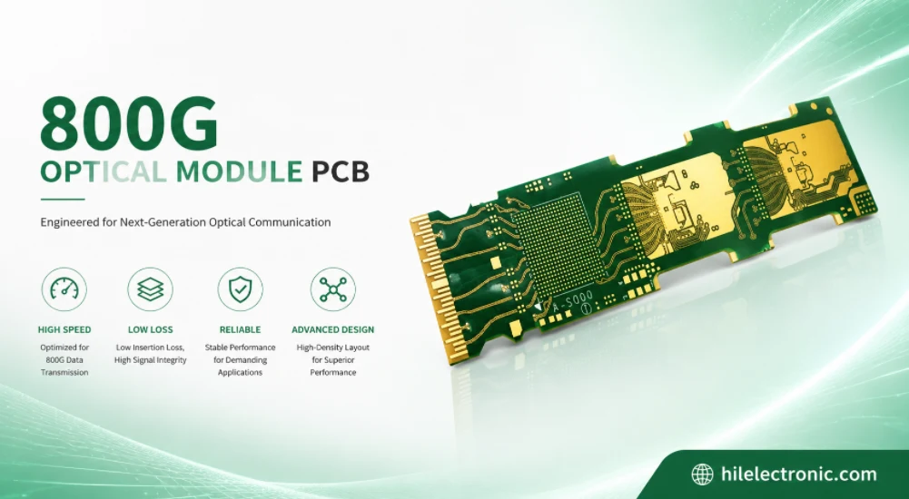
800G Optical Module PCB Manufacturing and Assembly Service
Table of contentsWhat Makes an 800G Optical Module PCB...
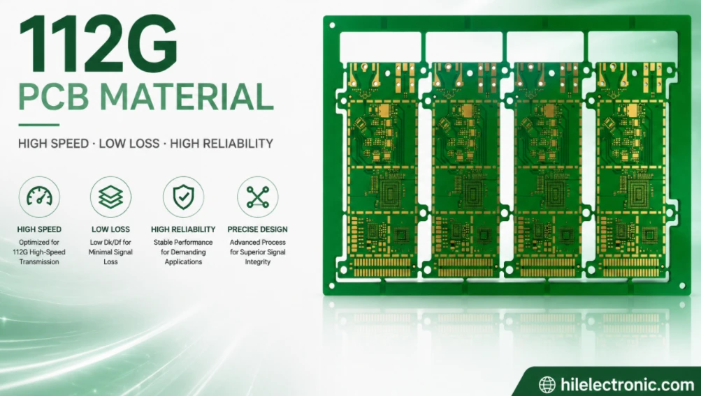
112G PCB Material Selection and High-Speed PCB Manufacturing
Table of contentsWhat “112G PCB Material” Actually...
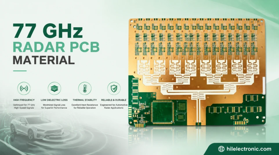
77 GHz Radar PCB Material Selection and Manufacturing Guide
Table of contentsWhat 77 GHz Changes in a PCBCommon 77 GHz...
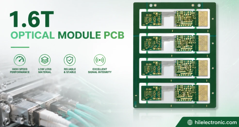
1.6T Optical Module PCB Manufacturing and Assembly Service
Table of contents1.6T Module Architectures and PCB...
How to get a quote for PCBs
Let us run DFM/DFA analysis for you and get back to you with a report.
You can upload your files securely through our website.
We require the following information in order to give you a quote:
-
- Gerber, ODB++, or .pcb, spec.
- BOM list if you require assembly
- Quantity
- Turn time
In addition to PCB manufacturing, we offer a comprehensive range of electronic services, including PCB design, PCBA (Printed Circuit Board Assembly), and turnkey solutions. Whether you need help with prototyping, design verification, component sourcing, or mass production, we provide end-to-end support to ensure your project’s success. For PCBA services, please provide your BOM (Bill of Materials) and any specific assembly instructions. We also offer DFM/DFA analysis to optimize your designs for manufacturability and assembly, ensuring a smooth production process.