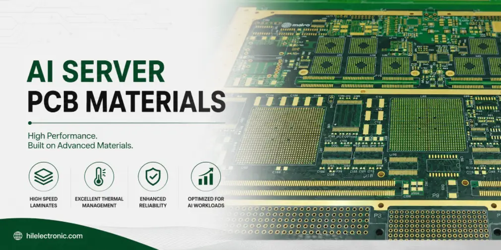
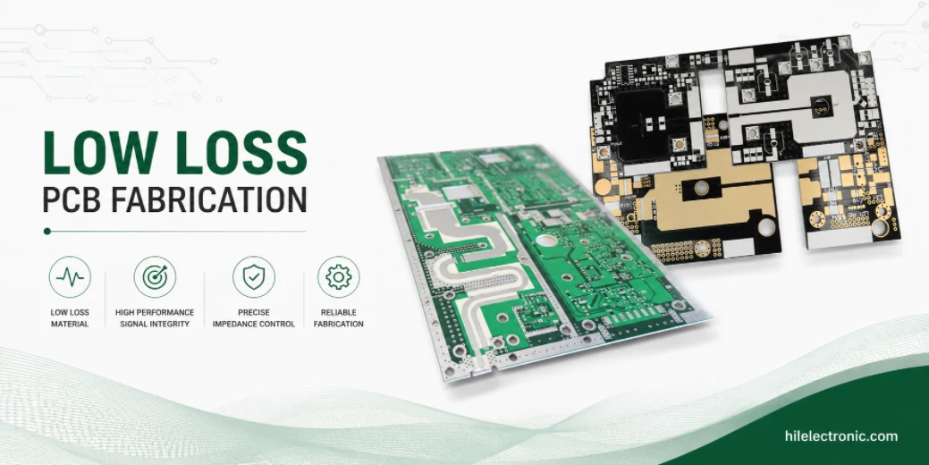
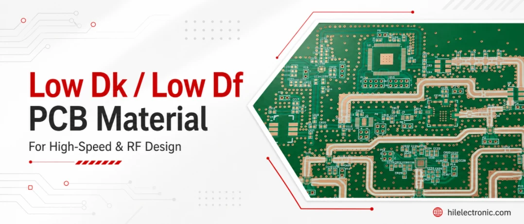
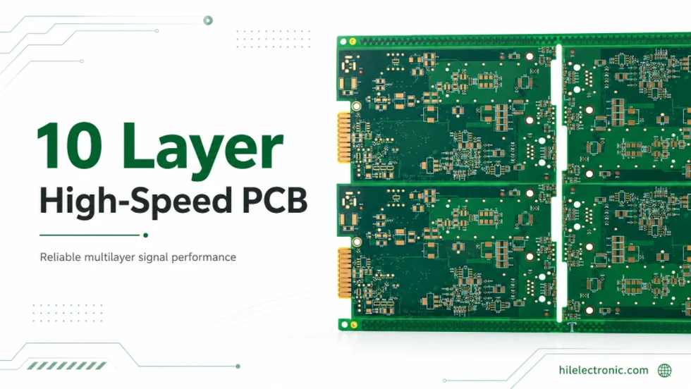
Select Page

Your PCB Manufacturing Expert – Highleap Electronic

High Speed PCB Material Selection for Signal Integrity

High Speed PCB Material Selection for Signal Integrity

Figure 1. High speed PCB material selection. On this page Material Properties That Matter Understanding Dk, Df, Tg, and CTE When FR4 Is No Longer Suitable Material Choices for AI and Networking Hardware Stack-Up Planning Considerations Manufacturer Review Before...

High Layer Count PCB Materials for Multilayer Boards

High Layer Count PCB Materials for Multilayer Boards

Table of contents Material Requirements for High Layer Count Designs Core and Prepreg Selection Lamination Yield Considerations Managing Warpage and Registration Material Lead Time Challenges Manufacturer Stack-Up Review Process High Layer Count PCB Materials FAQs A...

Low Loss PCB Fabrication for High-Speed Digital and RF Applications

Low Loss PCB Fabrication for High-Speed Digital and RF Applications

On this page What Is Low Loss PCB Fabrication When Do You Need Low Loss PCB Fabrication Low Loss PCB Materials Commonly Used in Manufacturing Low Loss PCB Manufacturing Capabilities How to Reduce Risk Before Ordering a Low Loss PCB Choosing a Low Loss PCB Manufacturer...

Low Dk Low Df PCB Material for High Speed Signals

Low Dk Low Df PCB Material for High Speed Signals

Figure 1. Low loss PCB material selection for high speed boards. On this page What Low Dk and Low Df Mean Signal Loss Reduction Benefits Comparing Low Dk Materials to FR4 Manufacturing Considerations Cost and Lead Time Factors Low Dk Low Df Material FAQs Two numbers...

10 Layer High-Speed PCB Engineering for DDR5 and PCIe

10 Layer High-Speed PCB Engineering for DDR5 and PCIe

Figure 1. 10 layer high-speed PCB for DDR5 and PCIe routing. Table of Contents Start with the Channel, Not the Protocol Label What the Data Rate Does-and Does Not-Tell You Build an Insertion-Loss and Discontinuity Budget Select Material, Copper and Geometry Together...

10 Layer PCB Impedance Control and TDR Verification

10 Layer PCB Impedance Control and TDR Verification

Figure 1. 10 layer PCB impedance control coupon and TDR verification. Table of Contents Controlled Impedance Is a Stackup and Process Definition Inputs Required Before Trace Geometry Can Be Released Single-Ended, Odd-Mode and Differential Impedance Microstrip,...

10 Layer PCB Stackup Design for Impedance and Planes

10 Layer PCB Stackup Design for Impedance and Planes

Figure 1. 10 layer PCB stackup for impedance and plane planning. Table of Contents Choose a Layer Architecture Before Choosing Dielectric Thickness Three Useful 10 Layer Stackup Archetypes A Reference-Plane-Rich 10 Layer Example Press-Out, Copper and Impedance Closure...

10 Layer PCB Routing Rules for DDR5, PCIe and Crosstalk

10 Layer PCB Routing Rules for DDR5, PCIe and Crosstalk

Figure 1. 10 layer PCB routing rules for DDR5 PCIe and crosstalk. Table of Contents Freeze the Electrical Rules Before Routing Begins Layer Assignment and Return-Path Continuity Differential Pairs: Geometry, Skew and Transitions DDR5 and Other Parallel Memory...

10 Layer PCB Manufacturer for Rigid, Flex and Rigid-Flex

10 Layer PCB Manufacturer for Rigid, Flex and Rigid-Flex

Figure 1. 10 layer PCB manufacturer production capability. Table of Contents 10 Layer PCB Manufacturer for Rigid, Flex and Rigid-Flex Boards How to Choose a 10 Layer PCB Manufacturer 10 Layer PCB DFM, Material Selection and Design Support Before Production 10 Layer...