
Panasonic R-5785(N) MEGTRON 7 PCB Manufacturer and Fabrication
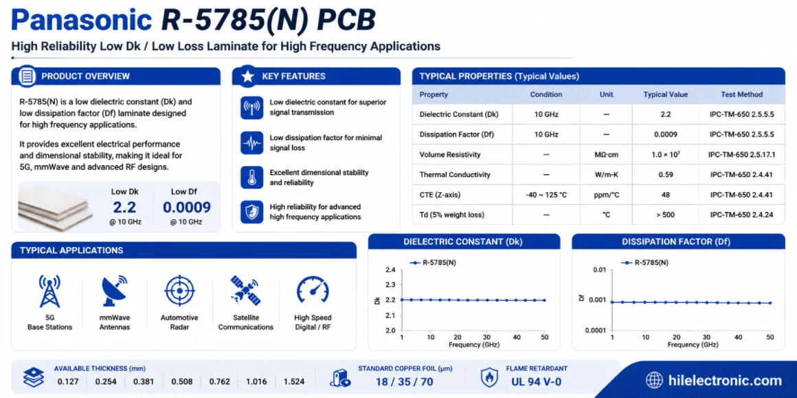
Highleap Electronics reviews, fabricates, and assembles Panasonic R-5785(N) MEGTRON 7 PCBs for AI server PCB material selection, high-capacity switches, routers, backplanes, test systems, and other long high-speed channels. We connect R-5785(N) laminate, R-5680(N) prepreg, low-Dk glass, copper profile, vias, assembly, and channel-test requirements in one production release.
R-5785(N) PCB Manufacturing for Advanced Interconnect
Highleap supports R-5785(N) MEGTRON 7 PCB builds for demanding high-speed channels, including high-layer multilayers, controlled impedance, back drilling, fine-pitch BGA breakout, sequential lamination, and advanced interconnect. Any-layer interconnect and other exceptional structures can be reviewed when the complete stackup, microvia hierarchy, reliability targets, material source, and expected yield are available; standard published examples are not a ceiling on reviewed projects.
Important: Highleap supports engineering samples, qualification runs, and stable volume production. Special material, interconnect, or signal-integrity requirements should be submitted with the RFQ so the fabrication and assembly route can be confirmed before release.
Best fit
Long, loss-limited channels in AI servers, switches, routers, backplanes, storage, and high-speed test platforms.
Main mistake
Choosing the highest material grade while ignoring copper roughness, via stubs, connectors, breakout, and the exact purchasable construction.
Highleap scope
Material/supply verification, stackup, H-VLP copper review, impedance/loss coupons, high-layer-count processing, back drilling, PCBA, and testing.
Quote inputs
Channel budget, R-5785(N)/R-5680(N) construction, copper, stackup, vias/back drill, dimensions, quantity/forecast, assembly, and test files.
When a Design Should Move to R-5785(N) / MEGTRON 7
Panasonic R-5785(N) is a MEGTRON 7 laminate used with R-5680(N) prepreg. Panasonic positions the family as an ultra-low-transmission-loss, high-heat-resistance system; the “N” construction uses low-Dk glass, and H-VLP copper options are associated with reducing conductor loss.
Upgrade is justified when
- MEGTRON 6N or another approved material leaves insufficient insertion-loss or eye margin;
- long server, switch, backplane, AI, or test channels remain limited after via and connector optimization;
- low-Dk glass and very-low-profile copper are included in the actual channel model;
- the business value of added margin exceeds material and qualification cost.
Upgrade is not justified when
- the channel already passes with stable production margin;
- the limiting loss comes from connectors, packages, stubs, or routing discontinuities;
- the design assumes a copper profile or glass construction that will not be purchased;
- the project has no defined loss or margin acceptance criterion.
The correct question is not “Is MEGTRON 7 better?” It is “What measurable product margin do we gain, and can the approved construction be procured and manufactured repeatedly?”
Highleap R-5785(N) Manufacturing and Assembly Scope
Highleap can review R-5785(N) high-layer-count rigid multilayers for prototypes, engineering builds, and volume production. The service can include R-5680(N) prepreg planning, controlled impedance, loss coupons, H-VLP copper review, back drilling, HDI, press-fit, component sourcing, SMT/through-hole assembly, large-BGA X-ray, and customer-defined functional or channel testing.
| Capability area | What is reviewed | Why it matters commercially |
|---|---|---|
| Exact material construction | R-5785(N), R-5680(N), low-Dk glass, copper profile, thickness, resin content, regional supply, MOQ, and traceability. | Prevents quoting a family name that cannot be purchased in the required form. |
| Channel-preserving stackup | Signal-reference pairs, actual Dk/Df basis, glass style, pressed thickness, finished copper, roughness, impedance, and coupons. | Ensures the fabricated board represents the customer’s SI model. |
| High-layer-count process | Press cycles, copper balance, registration, drilling, plating, warpage, board size, and panel utilization. | Establishes yield, cost, and lead-time risk. |
| Via/back-drill architecture | Residual stub, depth tolerance, pad/antipad, aspect ratio, filled vias, sequential lamination, and verification. | Stops via discontinuities from erasing the material benefit. |
| PCBA and production release | BGA warpage, press-fit, connectors, thermal hardware, reflow, inspection, functional test, and traceability. | Creates one accountable PCB-to-PCBA manufacturing plan. |
Final capability is always project-specific. Layer count alone does not define difficulty; the interaction of thickness, dimensions, hole range, copper, press cycles, tolerances, and test determines the route.
Design and RFQ Inputs for Ultra-Low-Loss Channels
An R-5785(N) quotation should be built from the channel and the production stackup. The buyer should provide more than “MEGTRON 7” and a layer count.
Electrical package
- interface standards, data rates, rise times, topology, and maximum physical channel lengths;
- single-ended and differential impedance targets and tolerances;
- insertion-loss, return-loss, crosstalk, skew, eye, or COM requirements and frequency basis;
- package, connector, via, and routing assumptions used in simulation;
- copper profile/roughness and glass construction used in the model;
- back-drill and residual-stub requirements;
- coupon design, fixture, calibration, de-embedding, and pass/fail limits.
Mechanical and production package
- complete fabrication data, drawing, netlist, dimensions, thickness, warpage, and panel requirements;
- core/prepreg construction, copper weights, resin-fill assumptions, and allowed alternatives;
- quantity by revision, prototype plan, annual forecast, delivery target, quality class, and traceability;
- BOM, placement, assembly drawings, press-fit, heat-sink/stiffener, test, and programming requirements.
Highleap can propose a production stackup, but any departure from the customer’s simulated construction must be reviewed before approval.
How Low-Dk Glass and H-VLP Copper Preserve Margin
Ultra-low-loss laminate is only one term in the channel equation. The practical manufacturing review separates the major loss sources.
Dielectric loss
Controlled by resin/glass chemistry, frequency, resin content, dielectric thickness, temperature, and field distribution. R-5785(N) is selected to reduce this contribution.
Conductor loss
Controlled by copper profile, skin effect, trace width, finished copper, current crowding, surface finish, and modelling method. Pairing an ultra-low-loss dielectric with unnecessarily rough copper wastes part of the benefit.
Discontinuity loss
Created by pads, anti-pads, vias, residual stubs, connectors, packages, reference-plane changes, neck-downs, and breakout geometry. Back drilling or a better via transition may produce more margin than another material change.
Manufacturing variation
Pressed thickness, etched width, plating growth, registration, glass distribution, and resin content create lot-to-lot variation. Representative coupons and first-article correlation are required if the product depends on a narrow margin.
The factory should report what it controls and avoid implying that a laminate datasheet guarantees the system eye diagram.
High-Layer-Count Fabrication and Production Qualification
- Material availability review. Confirm exact R-5785(N)/R-5680(N) constructions, copper, lead time, MOQ, and approved supply source.
- Stackup and resin-fill planning. Select purchasable cores and prepregs, balance copper, estimate pressed thickness, and maintain symmetry.
- Lamination and registration. Define press cycles, scaling, tooling, interlayer alignment, and thermal history.
- Drilling, back drilling, and plating. Control hole quality, aspect ratio, residual stubs, press-fit fields, plated copper, and verification coupons.
- Etch and impedance control. Correlate line compensation to actual foil and finished copper, then verify the agreed coupon method.
- Assembly qualification. Review moisture, reflow count, board support, BGA/connector coplanarity, press-fit, heat sinks, and warpage.
- Release evidence. Link material lots, travelers, electrical test, microsections, impedance/loss results, X-ray, functional test, and deviations to the shipment.
Production qualification should use the same material construction and acceptance method as the prototype. A prototype on a different copper profile or glass construction does not prove volume-channel performance.
R-5785(N) Cost, Supply, and Lead-Time Factors
| Driver | Commercial impact | Management action |
|---|---|---|
| Exact core/prepreg/copper construction | Premium or uncommon combinations can have MOQ, allocation, and extended procurement. | Confirm supply before final layout and maintain a controlled forecast. |
| Layer count and dimensions | Material usage, press complexity, registration, drilling, plating, panel yield, and warpage increase. | Optimize layer count and panel size with the fabricator. |
| Tight loss/impedance tolerance | Requires stricter process windows, coupons, first-article data, and potential yield loss. | Define realistic limits tied to system margin. |
| Back drill, HDI, and press-fit | Additional drilling, lamination, fill, depth verification, and reliability testing add cost. | Use only where the channel or breakout requires it. |
| Large BGA and mechanical hardware | Assembly support, X-ray, warpage control, heat-sink and connector operations can dominate PCBA cost. | Include mechanical and assembly data in the first RFQ. |
| Qualification and reporting | VNA fixtures, calibration, environmental tests, data packs, and traceability increase engineering time. | Agree sample sizes and acceptance evidence before release. |
Highleap provides a firm schedule after material, CAM, fabrication, assembly, and testing have been reviewed. Ultra-low-loss boards should also include a material-planning strategy for repeat orders.
Why Choose Highleap for MEGTRON 7 Production?
Highleap’s value is the conversion of an electrical requirement into a controlled manufacturing release. The service can include material verification, stackup engineering, high-layer-count fabrication, impedance and loss coupons, back drilling, HDI, PCB assembly, press-fit, inspection, functional test, and traceability.
The production response should answer the buyer’s real questions: Is the exact construction available? Which geometry will be fabricated? Which risks remain? What data will be measured? What changes require approval? What drives price and lead time? Can the same process move from prototype to volume?
For comparison and planning, see the MEGTRON 7 material guide, high-speed stackup guide, and backplane PCB manufacturing guide.
Commercial FAQ
Can Highleap manufacture Panasonic R-5785(N) / MEGTRON 7 PCBs?
Yes, suitable high-layer-count projects can be reviewed for fabrication and assembly. Final feasibility depends on the exact material construction, copper, layer count, thickness, dimensions, vias, tolerances, quantity, and tests.
Is R-5785(N) the MEGTRON 7 laminate?
Yes. R-5785(N) is a MEGTRON 7 laminate designation, and R-5680(N) is the related prepreg used in multilayer constructions.
Should every AI server use MEGTRON 7?
No. The material should be selected when channel analysis shows a real need for additional loss margin. Short or optimized channels may meet requirements on MEGTRON 6N or another approved material.
Can MEGTRON 6N be substituted without redesign?
No automatic substitution is responsible. Loss, Dk/Df, copper profile, glass, thickness, impedance geometry, via behaviour, supply, and qualification may differ. Customer approval and revalidation are required.
What files are needed for price and lead time?
Send complete fabrication and assembly data, exact materials, stackup, copper profile, controlled-impedance and channel-loss criteria, via/back-drill table, dimensions, quantities, forecast, delivery, and test plan.

Recommended Posts

Taconic RF 35 vs RO4350B PCB
Table of contentsRF-35 vs RO4350B Procurement and...

TMM4 Filter PCB Manufacturing
TMM4 filter PCB manufacturing is controlled by the...

TMM3 PCB Manufacturing for RF Modules
TMM3 PCB manufacturing is most useful where the RF module...

TMM6 PCB Fabrication
TMM6 fabrication is the process-control page for a mid-Dk...
How to get a quote for PCBs
Let’s run DFM/DFA analysis for you and get back to you with a report. You can upload your files securely through our website. We require the following information in order to give you a quote:
-
- Gerber, ODB++, or .pcb, spec.
- BOM list if you require assembly
- Quantity
- Turn time
For PCBA services, please provide your BOM (Bill of Materials) and any specific assembly instructions. We also offer DFM/DFA analysis to optimize your designs for manufacturability and assembly, ensuring a smooth production process.