Select Page

Your PCB Manufacturing Expert – Highleap Electronic

Black Box PCB Reverse Engineering for Undocumented Boards

Black Box PCB Reverse Engineering for Undocumented Boards

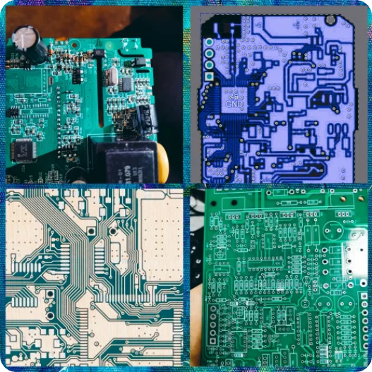
Figure 1. Black box PCB reverse engineering Table of Contents What Defines a Black Box PCB and Why Standard Methods Fall Short The Black Box Assessment: Determining What You Are Dealing With External Interface Analysis: Working from the Outside In Internal Analysis:...

PCB BOM Reconstruction Services | Extract BOM from Physical Board

PCB BOM Reconstruction Services | Extract BOM from Physical Board

Table of Contents What BOM Reconstruction Delivers and Why It Is Essential Component Identification: From Physical Marking to Verified Part Number The Complete BOM Reconstruction Methodology Handling Obsolete, Discontinued, and Unmarked Components BOM Verification and...

Circuit Board Reverse Engineering Services

Circuit Board Reverse Engineering Services

Table of Contents Why Boards End Up Without Documentation What the Service Actually Produces The Hard Variables: What Slows a Project Down Firmware, ASICs, and What Cannot Be Recovered Cost and Timeline: What the Numbers Depend On How to Avoid Getting Locked In by the...

Electronic Reverse Engineering Service

Electronic Reverse Engineering Service

You send us a physical PCB — or an electronic product containing PCBs. Our electronic reverse engineering service converts it into a complete, verified manufacturing package: Gerber files, schematic diagram, Bill of Materials, netlist, pick-and-place data, and...

Multilayer PCB Reverse Engineering Services

Multilayer PCB Reverse Engineering Services

Table of Contents Why Multilayer PCB Reverse Engineering Matters Standards and Quality Requirements for Multilayer RE Legal, IP, and Data Security Boundaries Multilayer PCB Construction Characteristics The Multilayer PCB Reverse Engineering Methodology Supply Chain,...

HDI PCB Reverse Engineering for Manufacturing

HDI PCB Reverse Engineering for Manufacturing

Table of Contents What Makes High-Density PCBs the Most Difficult to Reverse Engineer HDI Technology Features and Their RE Challenges Imaging and Capture Methods for HDI Boards Reconstructing HDI Layouts: Microvias, Sequential Lamination, and Stackup BGA Component...

Comprehensive PCB Cloning Solutions in China

Comprehensive PCB Cloning Solutions in China

[pac_divi_table_of_contents title="On this article" default_state="closed" included_headings="off|on|off|off|off|off" exclude_headings_by_class="on" active_link_highlight="on" level_markers_3="icons" title_container_padding="10px|15px|10px|15px|true|false"...

Schematic Extraction: Converting PCBs to Readable Diagrams

Schematic Extraction: Converting PCBs to Readable Diagrams

[pac_divi_table_of_contents title="On this article" default_state="closed" included_headings="off|on|off|off|off|off" exclude_headings_by_class="on" active_link_highlight="on" level_markers_3="icons" title_container_padding="10px|15px|10px|15px|true|false"...

Circuit Board Reverse Engineering Services

Circuit Board Reverse Engineering Services

[pac_divi_table_of_contents title="On this article" default_state="closed" included_headings="off|on|off|off|off|off" exclude_headings_by_class="on" active_link_highlight="on" level_markers_3="icons" title_container_padding="10px|15px|10px|15px|true|false"...

Fast PCB Copying Services to Support Your Projects

Fast PCB Copying Services to Support Your Projects

[pac_divi_table_of_contents title="On this article" default_state="closed" included_headings="off|on|off|off|off|off" exclude_headings_by_class="on" active_link_highlight="on" level_markers_3="icons" title_container_padding="10px|15px|10px|15px|true|false"...