
Comprehensive PCB Cloning Solutions in China

PCB cloning solutions that go beyond basic circuit board copying. True PCB cloning encompasses reverse engineering, design optimization, component sourcing, and manufacturing – all delivered as an integrated service that eliminates the risks and inefficiencies of working with multiple vendors.
The PCB Cloning Industry’s Trust Problem
The PCB cloning market suffers from systematic trust issues that harm clients and damage industry reputation. Common deceptive practices include:
-
Progressive Pricing Escalation: Starting with unrealistic low quotes, then adding charges for “unforeseen complexities”
-
Deliverable Hostage Situations: Withholding complete files or introducing errors if clients don’t commit to manufacturing contracts
-
Technical Competency Gaps: Promising capabilities they cannot deliver, resulting in failed projects and wasted time
-
Poor Communication: Leaving clients uninformed about progress, problems, or realistic timelines
Highleap Electronics has built our reputation by eliminating these industry problems. Our integrated approach, transparent pricing, and commitment to client success ensures every PCB cloning project delivers exactly what you need, when you need it.
End-to-End PCB Cloning Methodology
Comprehensive Analysis
Our cloning process begins with thorough analysis of your target PCB:
Design Extraction
Using advanced reverse engineering techniques:
Design Optimization
Our manufacturing expertise enables design improvements:
Prototype and Validation
Before full production, we validate cloned designs:
Advanced Cloning Technologies
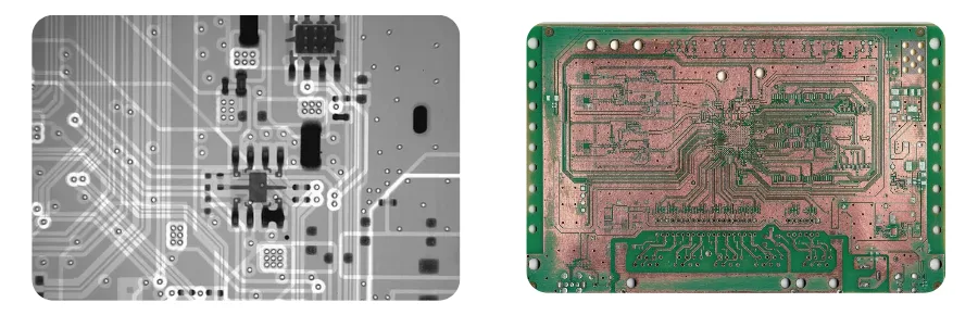
High-Resolution Imaging Systems
Our advanced imaging capabilities capture minute details:
-
Sub-micron resolution scanning
-
Multi-spectral imaging for layer visibility
-
3D profiling for component height mapping
-
Thermal imaging for thermal analysis
-
X-ray inspection for hidden structures
Automated Design Recognition
AI-assisted design recognition accelerates the cloning process:
-
Component pattern recognition
-
Trace routing optimization
-
Via structure analysis
-
Pad geometry extraction
-
Design rule compliance checking
These technologies work in conjunction with our capabilities to provide comprehensive system understanding.
Handling Complex PCB Architectures
Multi-Board Systems
Complex electronic products often require cloning entire PCB assemblies:
-
Main board and daughter card relationships
-
Connector specifications and mating
-
Cable and harness documentation
-
Mechanical integration requirements
-
System-level testing procedures
Advanced Technology Integration
Modern PCBs incorporate sophisticated technologies:
-
High-speed digital signals
-
RF and microwave circuits
-
Power electronics integration
-
Sensor interfaces and calibration
-
Communication protocol implementation
Component Sourcing and Supply Chain Management
Obsolescence Management
PCB cloning often involves replacing discontinued components:
-
Form-fit-function equivalent identification
-
Electrical characteristic matching
-
Qualification testing for substitutes
-
Supply chain reliability assessment
-
Long-term availability planning
Global Supply Network
Our extensive supplier relationships ensure component availability:
-
Authorized distributor partnerships
-
Independent distributor networks
-
Component manufacturer direct relationships
-
Specialized component sourcing services
-
Counterfeit component avoidance protocols
Integration with Specialized Services
Our PCB cloning solutions integrate seamlessly with related services. Complex projects benefit from our specialized applications and services for manufacturing documentation.
Complete system analysis is supported through for comprehensive technical understanding.
Why Choose Highleap Electronics for PCB Cloning
Our comprehensive approach eliminates the risks and inefficiencies of traditional PCB cloning:
- Transparent Pricing: Complete project costs defined upfront with no hidden charges
- Complete Deliverables: Full documentation and files regardless of manufacturing decisions
- Technical Excellence: Decades of experience in PCB design and manufacturing
- Integrated Services: Single-source solution from analysis through production
- Quality Assurance: Comprehensive testing and validation protocols
- Client Focus: Your success drives every decision we make
Start Your PCB Cloning Project Today
Don’t risk your critical PCB cloning project with providers who use deceptive practices or deliver compromised results. Choose Highleap Electronics for complete PCB cloning solutions you can trust.
Contact our technical team today to discuss your PCB cloning requirements. Experience the peace of mind that comes from working with true professionals committed to your success.

Related Articles

Rigid-Flex PCB for Robotics: Joint Interconnects That Survive Motion
Rigid-flex PCB manufacturing for robotics is valuable when...

HDI PCB for Robotics: Microvias, BGA Fanout and Signal Integrity
HDI PCB manufacturing for robotics is driven by compact...

Drone and Aerial Robot PCB for Flight Control and ESC Reliability
Drone and aerial robot PCB manufacturing is shaped by...

Collaborative Robot PCB for Cobot Safety and Joint Control
Collaborative robot PCBs support robots that operate near...
How to get a quote for PCBs
Let us run DFM/DFA analysis for you and get back to you with a report.
You can upload your files securely through our website.
We require the following information in order to give you a quote:
-
- Gerber, ODB++, or .pcb, spec.
- BOM list if you require assembly
- Quantity
- Turn time
In addition to PCB manufacturing, we offer a comprehensive range of electronic services, including PCB design, PCBA (Printed Circuit Board Assembly), and turnkey solutions. Whether you need help with prototyping, design verification, component sourcing, or mass production, we provide end-to-end support to ensure your project’s success. For PCBA services, please provide your BOM (Bill of Materials) and any specific assembly instructions. We also offer DFM/DFA analysis to optimize your designs for manufacturability and assembly, ensuring a smooth production process.