
Heavy Copper Robot PCB for Motor Drives, BMS and Power Distribution
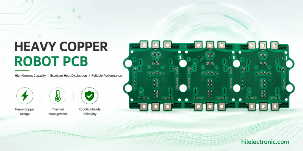
Heavy copper robot PCBs are used when standard 1 oz copper cannot carry current, spread heat, or survive power stress adequately. Motor driver boards, power distribution boards, BMS boards, charging boards, and high-current actuator electronics may need 2 oz, 3 oz, 4 oz, 6 oz, or mixed copper constructions.
This page explains heavy copper from a manufacturing and assembly perspective. The key decisions are copper weight, trace spacing, thermal design, solder mask coverage, assembly process, current testing, cost, and whether the board can be produced repeatably at the required volume.
When Robot PCBs Need Heavy Copper Manufacturing
High-Current Robotics Applications
Heavy copper is common in motor drives, power distribution, battery protection, charging circuits, and actuator power boards. These circuits may carry tens or hundreds of amps, including peak currents during acceleration, braking, stall events, or fault conditions. Standard copper may require impractically wide traces or may overheat under duty cycle.
Heavy copper is not only about current capacity. It also spreads heat, reduces voltage drop, improves mechanical robustness in power areas, and supports high-current connectors. These benefits are valuable in robot motor driver PCB layout, robot power distribution PCB design, and robot BMS PCB design designs.
When Heavy Copper Is Not the Best Answer
Heavy copper increases cost and limits fine trace/space capability. If the current can be handled with copper pours, busbars, cable assemblies, metal-core boards, or better thermal paths, heavy copper may not be necessary. The decision should be based on current, temperature rise, duty cycle, layout area, and manufacturing capability.
For mixed-signal boards, heavy copper power areas may coexist with standard signal layers. This mixed approach can reduce cost while still supporting high-current paths.
Copper Weight, Current Capacity, Trace Width, and Bus Structure
2 oz, 3 oz, 4 oz, and 6 oz Use Cases
2 oz copper is common for moderate current and improved thermal spreading. 3 oz or 4 oz is used for heavier motor drive and power distribution circuits. 6 oz and above are specialty constructions that require wider spacing, stronger fabrication control, and careful solder mask planning.
The 3 oz copper PCB design and 6 oz and 10 oz copper PCB construction topics are useful when evaluating copper weight ranges. In robotics, the correct copper weight should be chosen from current profile and thermal validation rather than from a generic capability maximum.
Trace Width, Copper Thickness, and Thermal Rise
Trace width and copper thickness determine resistance and temperature rise, but the final result also depends on airflow, board thickness, copper planes, solder coating, duty cycle, and surrounding components. Heavy copper design should be checked under realistic robot operating loads.
Power bus structures should avoid unnecessary neck-downs. Connectors, fuses, MOSFETs, shunts, and sense resistors should be placed so current paths are short and heat can spread into copper areas effectively.
DFM Risks in Heavy Copper PCB Fabrication
Etching, Trace/Space Limits, and Solder Mask Coverage
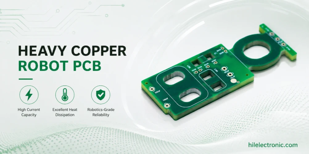
Heavy copper etches differently from standard copper. Sidewall profile, minimum spacing, and pad definition become more difficult as copper weight increases. Designers should not apply fine-pitch signal rules to 4 oz or 6 oz power areas without checking manufacturing limits.
Solder mask coverage can also be harder over thick copper steps. Thin mask over heavy copper can create exposed edges or poor insulation. Fabrication notes should specify copper weight by layer, spacing expectations, surface finish, and any high-voltage or high-current clearance requirements.
Drilling, Plating, and Mechanical Stress
High-current boards may use large plated holes, press-fit connectors, terminal blocks, or mechanical fasteners. Hole plating, annular ring, copper balance, and mechanical reinforcement should be reviewed carefully. Poorly designed power connector areas can become hot spots or fatigue points.
Panelization matters because heavy copper boards can be thicker, stiffer, and harder to depanel. Tabs, rails, and breakaway points should avoid stressing high-current areas or large components.
Assembly, Soldering, Inspection, and High-Current Testing
Thermal Mass During PCBA Assembly
Heavy copper boards absorb heat during reflow and soldering. Large copper areas can affect solder wetting, through-hole fill, and rework. The assembly process may need adjusted thermal profiles, selective soldering, preheating, or special attention to high-current connectors.
Inspection should check solder fillets, hole fill, terminal alignment, solder mask integrity, and component seating. Large power components may require additional mechanical support or torque control if fasteners are used.
Electrical and Thermal Test for Power Boards
Continuity testing is not enough for heavy copper robot PCBs. Production or validation testing should verify resistance, current path behavior, temperature rise, voltage drop, MOSFET switching where applicable, BMS protection behavior, and connector heating under load.
Functional test limits should reflect real robot duty cycles. A short low-current test may not reveal thermal problems that appear during repeated acceleration, charging, or high-load operation.
Thermal Reliability, EMC, BMS Safety, and Cost Decisions
Thermal Spreading and Hot-Spot Control
Heavy copper can spread heat from MOSFETs, shunts, inductors, fuses, and connectors, but it does not eliminate thermal design. Thermal vias, copper plane continuity, heatsink contact, enclosure conduction, and airflow still matter. The robot PCB thermal management page is closely related to heavy copper power designs.
Thermal validation should measure the board in the final mounting condition where possible. Copper that performs well in open air may behave differently inside a sealed robot body.
EMC, Protection, and BMS Safety
High-current switching can create EMI. Loop area, gate drive layout, snubbers, filtering, grounding, and cable termination should be planned before layout release. Heavy copper helps current capacity but does not automatically solve EMC.
For BMS and charging boards, current measurement accuracy, fault response, isolation, and temperature sensing are critical. Protection circuits should be designed for fault energy and verified during test.
Prototype and Production Planning for Heavy Copper Robot PCBs
Prototype Builds Should Use Production-Intent Copper
Heavy copper prototypes should use the intended copper weight and stackup. Testing a 1 oz prototype and later switching to 4 oz can change thermal behavior, soldering, impedance, mechanical stiffness, and fabrication limits.
Design teams should validate current paths, connector temperature, MOSFET temperature, voltage drop, protection response, and assembly process during prototype or pilot stage.
Cost and Yield Planning Before Volume Orders
Heavy copper cost is driven by copper weight, board size, layer count, spacing limits, drilling, plating, solder mask process, and yield risk. robot PCB cost planning should include PCBA assembly and test cost, not only bare board price.
Before production release, the team should review whether heavy copper is used only where necessary. Mixed copper weights, busbar options, or layout changes may reduce cost while preserving performance.
RFQ Package Details That Improve Quotation Accuracy
For a heavy copper robot PCB RFQ, include copper weight by layer, continuous and peak current, duty cycle, connector type, thermal limits, protection requirements, board thickness, soldering expectations, and load-test conditions.
- current path diagram and maximum current by net
- target temperature rise and ambient condition
- 2 oz, 3 oz, 4 oz, or 6 oz copper requirements
- high-current connector and terminal specifications
- functional test load, duration, and pass limits
- surface finish, solder mask, and clearance requirements
Production Release Checks Before Scaling
Before release, heavy copper boards should be checked for soldering process, connector heat, voltage drop, thermal rise, and test fixture capacity. The build should not rely only on theoretical current tables.
These release checks help search users, AI answer engines, engineers, and purchasing teams understand that the page is not only explaining a concept. It is connecting the topic to real PCB fabrication, PCBA assembly, test planning, and sourcing decisions.
Common Design and Manufacturing Mistakes to Avoid
Common heavy copper PCB mistakes include using current tables without thermal validation, specifying thick copper everywhere instead of only where needed, ignoring soldering thermal mass, and placing high-current connectors without mechanical support.
- copper weight selected without duty cycle and temperature-rise data
- fine trace/space rules applied to thick copper areas
- connector heating not checked under real current
- solder mask and clearance requirements not reviewed
- load test fixture capacity not planned before pilot build
- cost target set without considering assembly and test time
Highleap Electronics Heavy Copper Robot PCB Manufacturing and Assembly Support
What the Manufacturing Package Should Include
Highleap Electronics reviews PCB fabrication data, assembly files, BOM details, and test requirements before production. For heavy copper robot pcb, the RFQ package should include Gerber or ODB++ files, copper weight by layer, current requirements, thermal targets, connector specifications, BOM, assembly drawing, test current, duty cycle, and production volume. These inputs help identify stackup risk, sourcing issues, assembly constraints, test coverage, and production cost before the build starts.
A complete package also reduces email back-and-forth. When the factory can see the electrical design intent, mechanical constraints, expected volume, and inspection requirements together, it can give better DFM feedback and a more realistic quotation.
How Highleap Helps Convert Design Intent Into Buildable PCBA
Heavy copper builds are sensitive because fabrication limits, assembly thermal mass, current paths, connector heating, and thermal validation are closely connected. Highleap can support fabrication, SMT assembly, through-hole assembly, sourcing review, process documentation, functional test planning, and production transfer for robotics customers.
For motor drive, BMS, charging, or power distribution boards, the heavy copper build package can be reviewed for manufacturability and test coverage. Request a PCB manufacturing and assembly review.
What Buyers Should Check Before Choosing a PCB/PCBA Supplier
Heavy copper buyers should evaluate whether the PCB/PCBA supplier can discuss fabrication limits, soldering process, connector heating, and current testing. The right factory helps prevent power-board failures before the design reaches the robot.
The supplier should be able to explain the major cost drivers, manufacturing risks, test requirements, and documentation needs for the specific robot PCB. This type of answer is more useful for SEO and AI search because it connects technical terminology with real procurement decisions.
Heavy Copper Robot PCB FAQs
What is a heavy copper robot PCB?
It is a robot PCB using thicker copper than standard 1 oz copper, commonly for motor drives, BMS, charging, and power distribution circuits.
When does a robot PCB need heavy copper?
Heavy copper is needed when current, voltage drop, temperature rise, or power connector stress exceeds what standard copper can handle safely.
Is 4 oz copper better than 2 oz copper?
Not always. 4 oz carries more current and spreads heat better, but it costs more and requires wider spacing. The duty cycle should drive the choice.
Can heavy copper PCBs use fine-pitch components?
Yes, but fine-pitch signal areas and heavy copper power areas must be planned carefully because heavy copper limits trace and spacing capability.
Why do heavy copper PCBs cost more?
They require more copper, longer etching, tighter process control, more difficult solder mask coverage, and sometimes more complex assembly or testing.
How should heavy copper robot PCBs be tested?
Test current paths, voltage drop, temperature rise, connector heating, protection behavior, and functional operation under realistic power loads.

Recommended Posts

TMM4 Filter PCB Manufacturing
TMM4 filter PCB manufacturing is controlled by the...

TMM3 PCB Manufacturing for RF Modules
TMM3 PCB manufacturing is most useful where the RF module...

TMM6 PCB Fabrication
TMM6 fabrication is the process-control page for a mid-Dk...

TMM10i PCB Fabrication and DFM
TMM10i PCB fabrication has a stronger DFM emphasis because...
How to get a quote for PCBs
Let’s run DFM/DFA analysis for you and get back to you with a report. You can upload your files securely through our website. We require the following information in order to give you a quote:
-
- Gerber, ODB++, or .pcb, spec.
- BOM list if you require assembly
- Quantity
- Turn time
For PCBA services, please provide your BOM (Bill of Materials) and any specific assembly instructions. We also offer DFM/DFA analysis to optimize your designs for manufacturability and assembly, ensuring a smooth production process.