
Inside a China Ceramic PCB Factory: Process Control Across Power/LED/RF/Medical

Table of Contents
- Inside a China Ceramic PCB Factory: How Real Projects Move Through Production
- Power Electronics: IGBT Modules and EV Inverter Substrates
- LED Lighting: High-Brightness Thermal Substrates
- RF and Microwave: Precision Substrates for Signal Integrity
- Medical Devices: Compliance-Driven Ceramic PCB Production
- How Highleap Manages Multi-Industry Ceramic PCB Production
Most articles about ceramic PCBs talk about material properties and theoretical performance. This one focuses on something more practical: how a China ceramic PCB factory actually handles real projects across different industries — from the engineering review stage through production, testing, and delivery.
Every industry brings different requirements. A power module substrate for an EV inverter has completely different material, tolerance, and reliability demands than a ceramic board for an LED streetlight or a medical imaging sensor. A factory that tries to apply the same process to all of them will fail at most of them.
At Highleap Electronics, we handle ceramic PCB projects across power electronics, LED, RF/microwave, and medical segments — each with dedicated process parameters, inspection criteria, and documentation workflows. Here is how those projects differ in practice.
1. Inside a China Ceramic PCB Factory: How Real Projects Move Through Production
1.1 The Standard Workflow
Regardless of application, every ceramic PCB project follows a core production sequence:
- Engineering review: DFM analysis of customer files, material selection confirmation, process routing definition
- Substrate preparation: Incoming inspection, cleaning, lapping to required surface roughness
- Metallization: DBC bonding, thick-film printing, or thin-film deposition (depending on project)
- Circuit patterning: Photolithography, etching, laser trimming
- Post-processing: Surface finishing (ENIG, hard gold, Ni/Ag), laser scribing, singulation
- Inspection and testing: Dimensional, electrical, visual, and reliability testing per specification
- Assembly (if turnkey): SMT, wire bonding, die attach, encapsulation
- Final QC and shipping: CoC generation, packaging, logistics
1.2 Where Industry-Specific Requirements Diverge
The differences between industries are not in the sequence — they are in the specific parameters, tolerances, and documentation requirements at each step. The sections below illustrate these differences using representative project types.
2. Power Electronics: IGBT Modules and EV Inverter Substrates
2.1 Typical Requirements
| Parameter | Typical Specification |
|---|---|
| Substrate material | AlN or Si₃N₄ (for high thermal cycling) |
| Metallization | DBC, Cu thickness 0.3–0.6 mm |
| Current carrying | >100A per bus bar trace |
| Thermal cycling requirement | >3,000 cycles at –40°C / +150°C |
| Assembly | Die attach (solder or sintered silver), aluminum wire bonding |
| Certification | IATF 16949 (automotive); AEC-Q200 component qualification |
2.2 Factory Process Adaptations
Power module substrates demand the tightest process controls in ceramic PCB manufacturing. The DBC bonding step requires furnace temperature uniformity within ±3°C, with atmosphere composition monitored continuously. Post-bond copper etching must maintain trace width accuracy within ±50 µm to ensure proper current distribution across power bus structures.
The DBC substrate bonding process for power electronics also requires 100% X-ray or ultrasonic inspection of the copper-ceramic interface to detect voids that would create thermal hot spots under load.
For completed modules, our production line integrates multi-stage inspection including power cycling tests that simulate real inverter operating conditions before shipment.
3. LED Lighting: High-Brightness Thermal Substrates
3.1 Typical Requirements
| Parameter | Typical Specification |
|---|---|
| Substrate material | 96% Al₂O₃ (standard) or AlN (high-power) |
| Metallization | Thick film (Ag) or DBC |
| Surface finish | ENIG or hard gold (for wire bonding) |
| Reflectivity | >90% at 450 nm (for white-light LED packages) |
| Volume range | 1,000–100,000+ units per order |
3.2 Factory Process Adaptations
LED ceramic substrates prioritize consistent thermal conductivity and surface quality across large production volumes. The key challenge is maintaining substrate-to-substrate uniformity — because variation in thermal resistance directly translates to variation in LED junction temperature, which affects color consistency and lumen output across a lighting fixture.
For LED applications, the factory focus shifts toward high-volume consistency: SPC monitoring of substrate thickness and surface roughness across every production panel, automated screen printing with closed-loop paste thickness control for thick-film metallization, and 100% visual inspection for surface defects that could affect die-attach quality.
Our LED PCB solutions combine ceramic substrate fabrication with automated SMT assembly and optical testing to deliver fully characterized LED boards ready for system integration. For thermal design questions, our ceramic thermal management guide covers optimization strategies specific to LED applications.

4. RF and Microwave: Precision Substrates for Signal Integrity
4.1 Typical Requirements
- Substrate: 99.6% Al₂O₃ or AlN (selected for dielectric properties, not just thermal performance)
- Metallization: Thin film (sputtered Au or Cu, patterned photolithographically)
- Feature resolution: Line/space down to 25 µm for microstrip and CPW transmission lines
- Dielectric tolerance: Dk variation <±2% across the substrate area
- Surface finish: Electroless Ni/Au or thick Au for wire bonding
4.2 Factory Process Adaptations
RF ceramic PCBs demand the highest pattern resolution and the tightest dielectric control. The factory workflow for these projects includes thin-film deposition in cleanroom-grade environments (Class 1000 or better), photolithographic patterning with direct-imaging exposure for consistent trace geometry, and post-etch dimensional verification using automated optical measurement.
For projects requiring controlled impedance on ceramic, our engineers collaborate with customers on transmission line modeling before production — ensuring that the as-built trace dimensions achieve the target impedance within ±5%. This DFM step is especially critical because ceramic substrates do not offer the same stackup flexibility as multilayer FR4 or high-frequency laminate systems.
5. Medical Devices: Compliance-Driven Ceramic PCB Production
5.1 Typical Requirements
- Substrate: 96% or 99.6% Al₂O₃ (biocompatibility and long-term stability)
- Certification: ISO 13485 quality management system; full lot traceability
- Documentation: Device History Records (DHR), material certificates, inspection reports per unit
- Testing: Dielectric withstand, insulation resistance, functional test per device specification
- Handling: ESD protection, cleanroom packaging, moisture sensitivity management
5.2 Factory Process Adaptations
Medical ceramic PCB production is defined by documentation and traceability rather than extreme dimensional tolerances. Every substrate must be traceable to its raw material lot. Every process step must be recorded with operator ID, date, equipment serial number, and process parameters.
The factory must maintain ISO 13485 certification — not just ISO 9001 — and demonstrate that its CAPA (Corrective and Preventive Action) system is actively used, not just documented. Our PCB assembly operation supports medical builds with dedicated production tracking, serialized inspection records, and validated functional test procedures that satisfy regulatory submission requirements.
6. How Highleap Manages Multi-Industry Ceramic PCB Production
Operating as a China ceramic PCB factory serving multiple industries requires more than versatile equipment — it requires the ability to switch between different quality standards, documentation levels, and process parameters across concurrent production runs.
Highleap Electronics manages this through:
- Project-specific routing: Each ceramic PCB project receives a dedicated process traveler that specifies material, metallization parameters, inspection criteria, and documentation requirements — no two projects follow a generic default process
- Segregated production: Ceramic substrates are processed on dedicated lines separated from FR4 and metal-core production to prevent cross-contamination
- Multi-standard quality system: ISO 9001 + ISO 13485 + IATF 16949 + ISO 14001 — covering automotive, medical, and general industrial requirements simultaneously
- Integrated services: Full EMS capability from ceramic substrate fabrication through component sourcing, assembly, testing, and finished product delivery
Whether your project is a 20-piece prototype for a power module evaluation or a 10,000-unit production run for LED lighting, our process infrastructure adapts to your specific requirements — material, quality, and documentation.
Discuss Your Ceramic PCB Project
Contact our engineering team with your application requirements, and we will outline the specific process routing, materials, and testing plan for your project.
Shirley has 5 years of hands-on experience in PCB fabrication and assembly services. Her expertise includes complex multilayer boards, HDI structures, turnkey component sourcing, SMT assembly, testing, and full system integration. As both a technical advisor and sales specialist, she supports customers with DFM guidance, cost optimization, and production planning, helping projects move efficiently from design to mass production with consistent quality and on-time delivery.

Recommended Posts
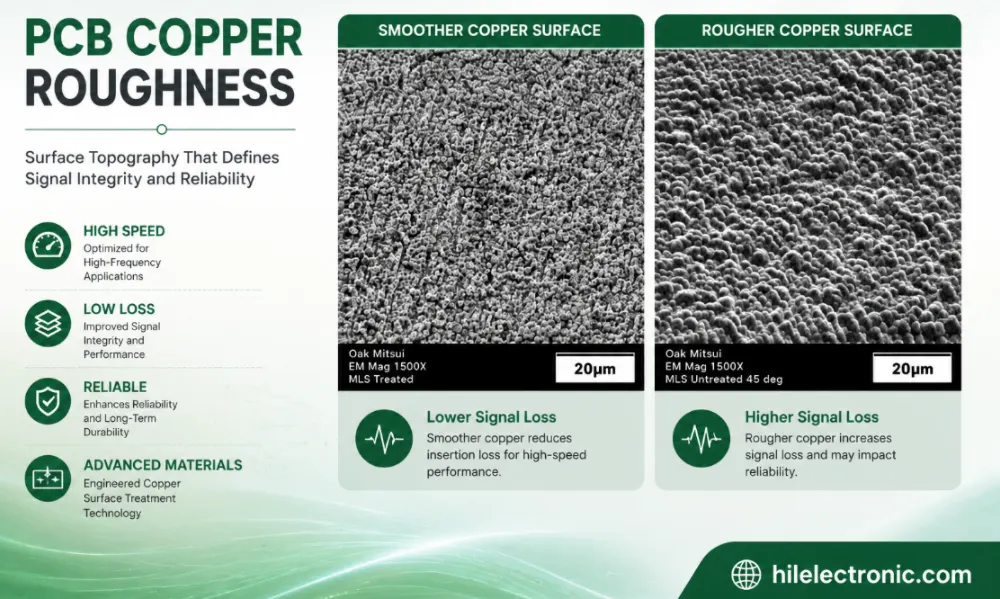
PCB Copper Roughness: Signal Loss, Material Selection and Manufacturing Control
Table of contentsWhat Is PCB Copper Roughness?How Copper...
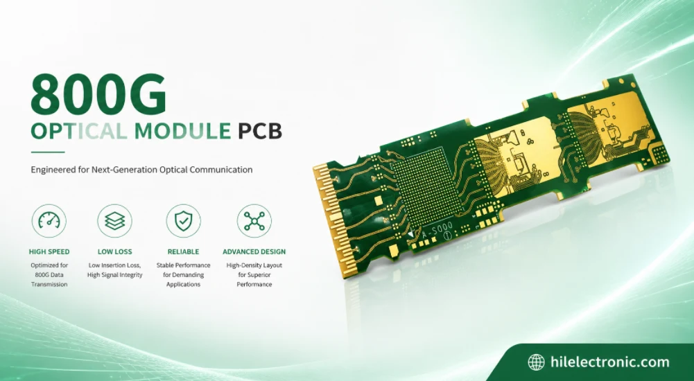
800G Optical Module PCB Manufacturing and Assembly Service
Table of contentsWhat Makes an 800G Optical Module PCB...
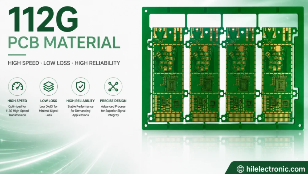
112G PCB Material Selection and High-Speed PCB Manufacturing
Table of contentsWhat “112G PCB Material” Actually...
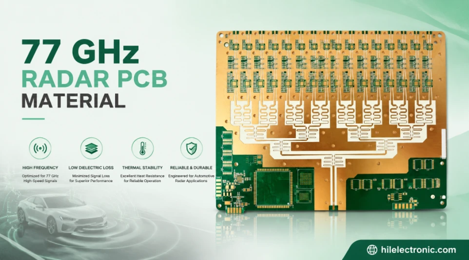
77 GHz Radar PCB Material Selection and Manufacturing Guide
Table of contentsWhat 77 GHz Changes in a PCBCommon 77 GHz...
How to get a quote for PCBs
Let us run DFM/DFA analysis for you and get back to you with a report.
You can upload your files securely through our website.
We require the following information in order to give you a quote:
-
- Gerber, ODB++, or .pcb, spec.
- BOM list if you require assembly
- Quantity
- Turn time
In addition to PCB manufacturing, we offer a comprehensive range of electronic services, including PCB design, PCBA (Printed Circuit Board Assembly), and turnkey solutions. Whether you need help with prototyping, design verification, component sourcing, or mass production, we provide end-to-end support to ensure your project’s success. For PCBA services, please provide your BOM (Bill of Materials) and any specific assembly instructions. We also offer DFM/DFA analysis to optimize your designs for manufacturability and assembly, ensuring a smooth production process.