
Ceramic PCB Thermal Management: Engineering Strategies for High-Power Applications

Why Ceramic PCB Thermal Management Defines High-Power Design Success
Ceramic PCBs have become essential substrates for high-power and high-density electronic applications including LED lighting systems, IGBT power modules, and RF amplifiers. These applications demand reliable heat dissipation to maintain performance and extend operational lifespan under continuous thermal stress.
The fundamental advantage of ceramic materials lies in their superior thermal conductivity compared to conventional FR4 laminates or standard metal-core boards. While aluminum-based PCBs typically offer thermal conductivity around 1-2 W/m·K, ceramic substrates like aluminum nitride and silicon nitride provide thermal performance ranging from 70 to 180 W/m·K.
This dramatic improvement enables direct thermal management at the substrate level rather than relying solely on external cooling solutions. Effective ceramic PCB thermal management design transforms substrate selection and stack-up architecture into critical engineering decisions that determine system reliability and performance headroom.
Material Selection: Foundation of Ceramic PCB Thermal Management
Understanding Thermal Conductivity Fundamentals
Thermal conductivity measures a material’s ability to transfer heat, directly influencing the thermal resistance between heat-generating components and heat sinks. Lower thermal resistance translates to reduced junction temperatures and improved device reliability. The relationship between thermal conductivity and thermal resistance follows an inverse proportion, where higher conductivity materials create shorter and more efficient thermal pathways.
Ceramic Material Performance Comparison
Different ceramic materials offer distinct thermal performance characteristics that align with specific application requirements:
- Alumina (Al₂O₃): 20-30 W/m·K – Cost-effective solution for moderate-power applications where thermal demands remain manageable and budget constraints favor economic material selection.
- Aluminum Nitride (AlN): 150-180 W/m·K – Premium material delivering exceptional thermal conductivity for high-power density designs requiring maximum heat dissipation capability.
- Silicon Nitride (Si₃N₄): 70-90 W/m·K – Intermediate thermal performance with superior mechanical strength and thermal shock resistance for demanding environmental conditions.
Material Selection Strategy for Thermal Management
The choice between ceramic materials depends on power dissipation requirements, operating temperature ranges, and coefficient of thermal expansion matching with semiconductor dies. AlN and Si₃N₄ exhibit CTE values closer to silicon at approximately 4-5 ppm/°C, reducing thermal stress during temperature cycling compared to alumina’s 6-8 ppm/°C.
The metallic layers bonded to ceramic substrates, typically copper ranging from 0.2mm to 0.6mm thickness, contribute significantly to lateral heat spreading. This copper metallization enables thermal distribution across larger substrate areas before vertical heat transfer through the ceramic base material to external heat sinks.

Thermal Pathway Design in Ceramic PCB Stack-Up Architecture
Heat Transfer Path Configuration
Effective ceramic PCB thermal management requires understanding the complete heat transfer pathway from semiconductor junction through solder interface, copper metallization, ceramic substrate, and finally to the heat sink or ambient environment. Each interface introduces thermal resistance that accumulates in series, making every layer optimization critical for overall thermal performance.
The thermal pathway design must balance electrical performance requirements with thermal efficiency to avoid creating hotspots or compromising signal integrity. Strategic placement of components and routing decisions directly impact how efficiently heat flows from generation points to dissipation mechanisms.
Direct Bonded Copper Technology
DBC technology creates a high-integrity bond between thick copper layers and ceramic substrates through a eutectic reaction at elevated temperatures. This process eliminates adhesive layers that would introduce additional thermal resistance in the critical heat transfer pathway.
DBC structures typically achieve copper thicknesses between 0.3mm and 0.6mm, providing excellent current-carrying capacity and heat spreading capability. The absence of intermediate materials makes DBC the preferred choice for ceramic PCB thermal management in power electronics exceeding 50W per component where thermal resistance minimization becomes paramount.
Direct Plated Copper Advantages
DPC manufacturing employs thin-film processes to deposit and pattern copper directly onto ceramic substrates. While copper thickness remains lower than DBC at typically 25-200μm, DPC enables finer feature resolution essential for high-density interconnects and complex circuit geometries.
The thinner copper layer slightly increases vertical thermal resistance but allows superior lateral heat distribution across larger substrate areas. DPC proves advantageous when ceramic PCB thermal management must accommodate densely packed components or complex routing requirements that exceed DBC patterning capabilities.
Multilayer Ceramic Thermal Optimization
LTCC and HTCC structures introduce vertical thermal challenges due to multiple ceramic layers in the stack-up. Strategic placement of thermal vias and internal metal planes creates parallel thermal pathways that compensate for increased substrate thickness.
Ceramic PCB thermal management in multilayer structures requires careful simulation to identify optimal via patterns. The goal remains maintaining thermal performance without compromising electrical design integrity or mechanical strength under thermal cycling conditions.
Thermal Simulation for Ceramic PCB Thermal Management Validation
Finite Element Analysis Implementation
Thermal simulation using finite element methods or computational fluid dynamics tools allows engineers to predict temperature distributions before prototyping. These simulations model heat generation sources, material properties, boundary conditions, and convective or conductive cooling mechanisms across the entire thermal management system.
Accurate modeling identifies potential thermal hotspots and validates whether the ceramic PCB thermal management design maintains junction temperatures within specified limits. Simulation results guide design iterations that optimize thermal performance before committing to expensive prototype fabrication.
Critical Modeling Parameters
Effective thermal modeling requires precise input data including actual power dissipation profiles, thermal interface material properties, and realistic boundary conditions representing the final assembly environment. Material property variations with temperature must be considered, as thermal conductivity typically decreases at elevated temperatures.
Contact resistance at solder joints and thermal interfaces often dominates the overall thermal resistance in ceramic PCB thermal management designs. These interface resistances require empirical validation through thermal test vehicle measurements rather than relying solely on theoretical calculations.
Balancing Thermal and Electrical Requirements
Ceramic PCB thermal management design frequently encounters trade-offs between optimal thermal pathways and electrical performance constraints. Wide copper traces that enhance heat spreading may introduce unwanted capacitance or inductance in high-frequency circuits where impedance control remains critical.
Thermal via placement must avoid disrupting controlled impedance transmission lines or creating return current discontinuities. Successful designs iterate between thermal and electromagnetic simulations to converge on solutions meeting both thermal dissipation and signal integrity specifications simultaneously.

Ceramic PCBs in Power Electronics and LED Applications
High-Power Application Design Solutions
LED Module Thermal Management
High-brightness LED modules concentrate significant heat flux in small junction areas, making ceramic substrates essential for preventing catastrophic thermal failure. AlN ceramic PCBs combined with DBC copper enable junction temperature reductions of 20-30°C compared to aluminum-core alternatives in equivalent operating conditions.
The ceramic PCB thermal management strategy often incorporates cavity-down mounting where LED dies attach directly to substrate metallization, minimizing thermal interface layers. This approach extends luminous flux maintenance and color stability throughout the operational lifetime by maintaining lower junction temperatures.
IGBT Power Module Requirements
Insulated-gate bipolar transistor modules in motor drives, renewable energy converters, and traction inverters generate heat densities exceeding 200 W/cm². Ceramic substrates, particularly Si₃N₄ with enhanced mechanical robustness, provide reliable thermal management under extreme temperature cycling from -40°C to 150°C.
The DBC structure supports high-current bus bar interconnections while maintaining low thermal resistance to the base plate. Power cycling capability improves significantly when ceramic PCB thermal management maintains junction temperatures within narrow operating windows, directly extending module lifetime.
Automotive Electronics Thermal Challenges
Automotive power control modules face demanding environmental conditions including wide temperature ranges, vibration, and long-term reliability requirements exceeding 15 years. Ceramic substrates offer stable thermal performance across temperature extremes that would degrade organic materials through delamination or thermal decomposition.
The coefficient of thermal expansion matching between ceramic and semiconductor materials reduces thermal stress accumulation during thousands of thermal cycles. Ceramic PCB thermal management proves critical in electric vehicle inverters where efficiency gains directly impact driving range and battery longevity through reduced cooling system requirements.
Conclusion: Integrated Engineering Approach
Successful ceramic PCB thermal management requires coordinated attention to material selection, structural design, and validation methodology. The thermal conductivity of the ceramic substrate establishes the performance ceiling, while stack-up architecture and metallization design determine how effectively that potential translates into practical thermal resistance reduction.
Modern high-power electronics demand thermal management solutions that go beyond traditional cooling approaches. As power electronics continue advancing toward higher switching frequencies and increased integration, ceramic PCB thermal management capabilities remain fundamental to enabling next-generation performance in increasingly compact form factors.
Highleap Electronics Ceramic PCB Thermal Management Capabilities
Highleap Electronics delivers comprehensive ceramic PCB manufacturing with integrated thermal design support:
- Material expertise – Engineering guidance on selecting optimal ceramic substrates matching your thermal and electrical requirements.
- DBC and DPC manufacturing – Advanced metallization processes delivering precise copper patterning with minimized thermal resistance.
- Thermal design validation – Simulation and testing services confirming thermal performance before volume production.
- High-reliability assembly – PCB assembly capabilities maintaining thermal interface integrity for demanding applications.
Partner with our engineering team to validate your ceramic PCB thermal management strategy and ensure reliable performance in high-power operating environments. Contact Highleap Electronics to discuss your next thermal management challenge.

Recommended Posts

RF Transceiver PCB Manufacturing and Assembly
Table of contentsRF Transceiver PCB Manufacturing and...
RFSoC Board PCB Manufacturing and Assembly One-Stop Service
Highleap Electronics supports customer-designed RFSOC...
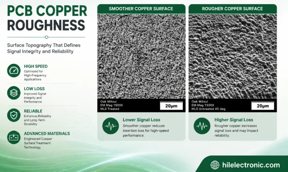
PCB Copper Roughness: Signal Loss, Material Selection and Manufacturing Control
Table of contentsWhat Is PCB Copper Roughness?How Copper...
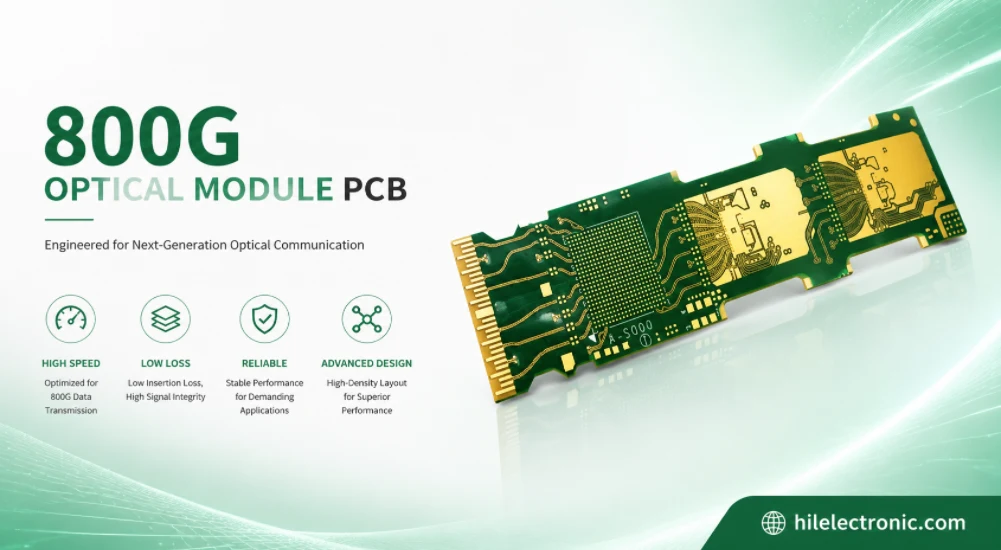
800G Optical Module PCB Manufacturing and Assembly Service
Table of contentsWhat Makes an 800G Optical Module PCB...
How to get a quote for PCBs
Let‘s run DFM/DFA analysis for you and get back to you with a report. You can upload your files securely through our website. We require the following information in order to give you a quote:
-
- Gerber, ODB++, or .pcb, spec.
- BOM list if you require assembly
- Quantity
- Turn time
In addition to PCB manufacturing, we offer a comprehensive range of electronic services, including PCB design, PCBA, and turnkey solutions. Whether you need help with prototyping, design verification, component sourcing, or mass production, we provide end-to-end support to ensure your project’s success.
For PCBA services, please provide your BOM (Bill of Materials) and any specific assembly instructions. We also offer DFM/DFA analysis to optimize your designs for manufacturability and assembly, ensuring a smooth production process.