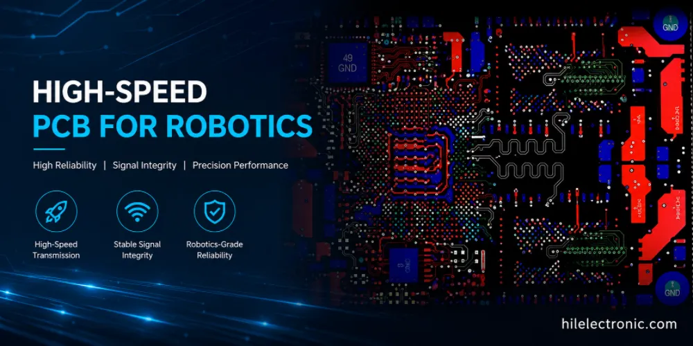
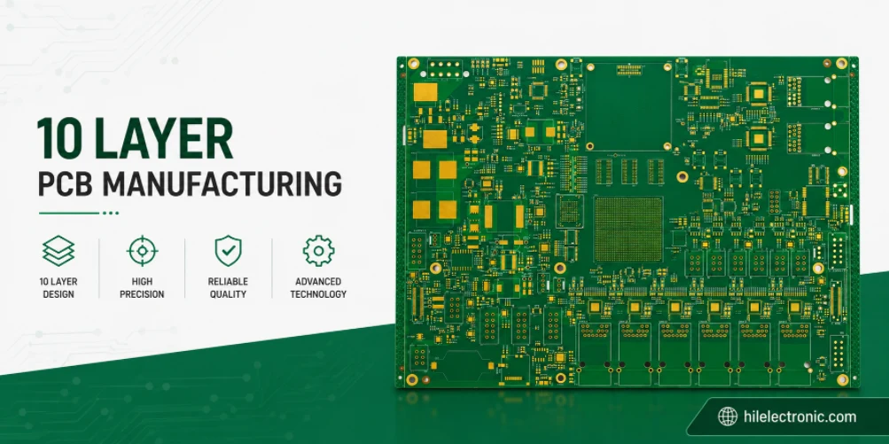
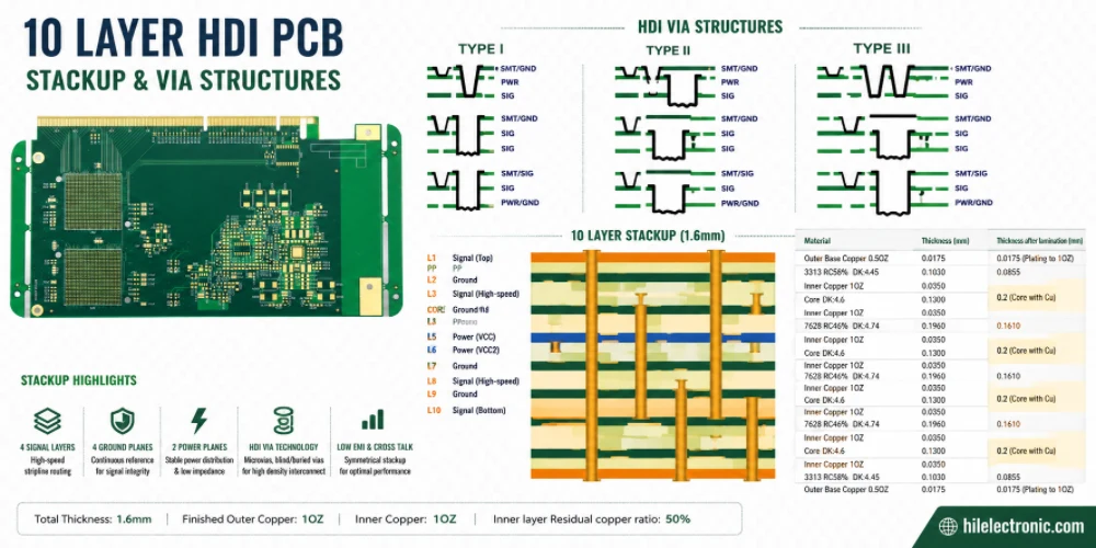
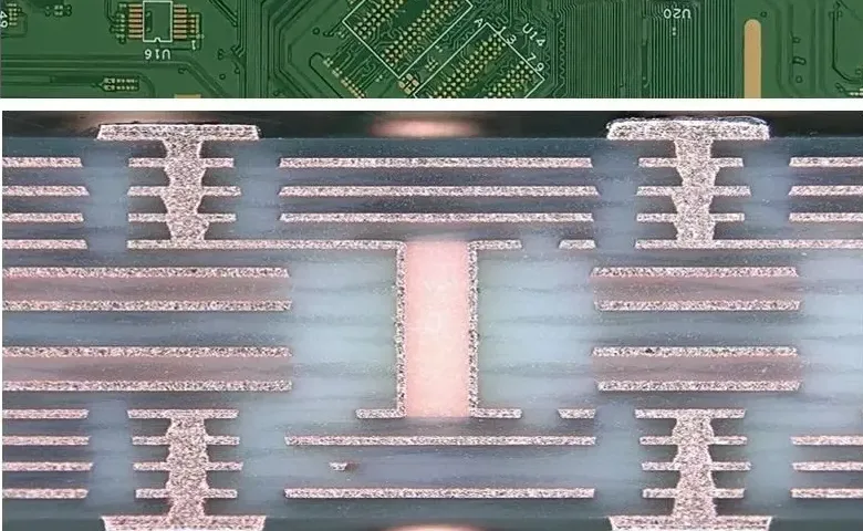
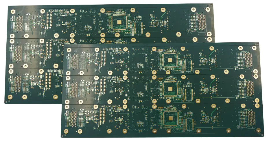
Select Page

Your PCB Manufacturing Expert – Highleap Electronic

10 Layer PCB Manufacturer for Rigid, Flex and Rigid-Flex

10 Layer PCB Manufacturer for Rigid, Flex and Rigid-Flex

Figure 1. 10 layer PCB manufacturer production capability. Table of Contents 10 Layer PCB Manufacturer for Rigid, Flex and Rigid-Flex Boards How to Choose a 10 Layer PCB Manufacturer 10 Layer PCB DFM, Material Selection and Design Support Before Production 10 Layer...

10 Layer HDI PCB Engineering for Microvias and BGA Escape

10 Layer HDI PCB Engineering for Microvias and BGA Escape

Figure 1. 10 layer HDI PCB engineering for microvias and BGA escape. Table of Contents When a 10 Layer Board Actually Needs HDI How to Read and Select 1+8+1, 2+6+2 and 3+4+3 Microvia Geometry, Capture Pads and Via-in-Pad Stacked, Staggered and Skip Microvias...

Blind Via PCB: Design Rules, Build Types, Cost and Guide

Blind Via PCB: Design Rules, Build Types, Cost and Guide

Figure 1.  PCB Design For Manufacturing Table of Contents What a Blind Via PCB Is — and What Makes It Different Three Scenarios Where Blind Vias Are the Correct Engineering Decision Blind Via Design Rules: Layer Pairing, Pad Size, Aspect Ratio, and Via-in-Pad HDI...

Laser Drilled PCB Vias Design Optimization and Costs

Laser Drilled PCB Vias Design Optimization and Costs

Figure 1. Laser drilling PCB Table of Contents When Does Your PCB Design Actually Need Laser Drilling? Microvia Design Rules: The Exact Numbers That Control Cost and Yield Aspect Ratio: The Single Most Expensive Mistake in HDI Design Via-in-Pad Rules and the Assembly...

Blind Via PCB Lamination Defect Prevention

Blind Via PCB Lamination Defect Prevention

Table of Contents Blind Via PCB Lamination: Sequential Build vs. Single-Cycle Process Lamination Cycle Requirements by HDI Type Pre-Lamination Preparation: Inner Layer and Material Requirements Lamination Press Cycle: Parameters, Phases, and Process Control...

Reduce Your 10-Layer Blind Buried Via PCB Cost

Reduce Your 10-Layer Blind Buried Via PCB Cost

Table of Contents What Actually Drives 10-Layer HDI Cost Beyond Layer Count Back-Drilling: The Signal Integrity Cost Decision Unique to High-Layer HDI Power Plane Architecture and Its Hidden Cost Impact Material Selection: Hybrid Stackup Strategy for 10-Layer 10-Layer...

8-Layer Blind Buried Via PCB Price Breakdown

8-Layer Blind Buried Via PCB Price Breakdown

Table of Contents 8-Layer Blind Buried Via PCB Price by Stackup Configuration How Stackup Choice Controls Price: Type I vs. Type II vs. Type III Via Count and Architecture: The Most Controllable Cost Variable Volume Pricing Curves for 8-Layer HDI NRE and Tooling for...

How to Design Fast Turnaround Blind Buried Via PCBs

How to Design Fast Turnaround Blind Buried Via PCBs

Table of Contents Fast Turnaround Blind Buried Via PCB: What's Actually Achievable The Lamination Time Floor: What Expediting Can and Cannot Compress Design Strategies That Enable Fast Turnaround Without Expedite Fees Specification Choices That Compress Processing...

How to Reduce Your Blind Buried Via PCB Lead Time

How to Reduce Your Blind Buried Via PCB Lead Time

Table of Contents Blind Buried Via PCB Lead Time: Standard Benchmarks by HDI Type Why Sequential Lamination Creates Non-Compressible Time Floors Lead Time by HDI Type: Process Timelines and Bottlenecks Material Availability: The Largest Lead Time Variable Design...