
Blind Via PCB: Design Rules, Build Types, Cost and Guide

Figure 1. PCB Design For Manufacturing
Table of Contents
- What a Blind Via PCB Is — and What Makes It Different
- Three Scenarios Where Blind Vias Are the Correct Engineering Decision
- Blind Via Design Rules: Layer Pairing, Pad Size, Aspect Ratio, and Via-in-Pad
- HDI Build Type Selection: Which One Your Design Actually Needs
- Stacked vs. Staggered Microvias: Reliability Data and Design Tradeoffs
- Blind Via PCB Cost: Drivers, Multipliers, and What Designers Can Control
- Evaluating a Blind Via PCB Manufacturer: The Questions That Reveal Capability
A blind via PCB is a circuit board in which one or more vias connect an outer copper layer to a specific inner layer without penetrating the full board thickness. The hole starts at the surface and stops — precisely — on the target inner copper, which acts as the physical termination surface during laser drilling. That single physical property separates blind via PCBs from standard multilayer boards in three consequential ways: the via occupies only the layers it connects rather than consuming routing space across all layers; the pad diameter is smaller (typically 0.25–0.35mm versus 0.50–0.70mm for through-hole), enabling fanout geometry that is geometrically impossible with mechanical drilling; and the via has no unused copper stub below the signal exit layer, eliminating the quarter-wave stub resonances that degrade channels above 10 Gbps. This guide is written for hardware engineers, PCB designers, and sourcing engineers who need to make real decisions about blind via PCBs — whether to use them, which build type to specify, which design rules are non-negotiable, and what separates a capable manufacturer from one that will fail at volume.
What a Blind Via PCB Is — and What Makes It Different
The Three Via Structures in HDI Boards
| Via Type | Span | Formation Method | Typical Finished Diameter | Primary Application |
|---|---|---|---|---|
| Through-hole via | Full board thickness, all layers | Mechanical drill, single lamination | 0.20–0.50mm | Power, ground, signals on ≥0.65mm pitch BGAs |
| Blind via (microvia) | Outer layer to one specific inner layer | Laser drill after outer buildup lamination | 0.075–0.15mm | Fine-pitch BGA fanout; stub-free high-speed routing |
| Buried via | Inner layer to inner layer only | Mechanical drill on sub-core before outer lamination | 0.20–0.30mm | Dense inner routing; freeing outer layers for components |
Why Blind Vias Increase Routing Density
On a standard 10-layer board, a through-hole via carries a signal from L1 to L2 but occupies pad space on all 10 layers. Every layer it passes through loses a routing channel for every via in the design. With 200 through-hole signal vias on a dense board, the routing penalty compounds across the entire layer stack.
A blind via from L1 to L2 uses only those two layers. The remaining eight layers have no pad obstruction from that via at all. Combined with the smaller pad diameter — a 0.10mm blind via with a 0.30mm land pad versus a 0.30mm drill with a 0.60mm pad for a standard signal via — this is what makes 0.50mm and 0.40mm pitch BGA fanout physically achievable. At those pitches, the geometric constraint is absolute: the pad-plus-annular-ring diameter of a through-hole via exceeds the pitch spacing, so a blind via is not a performance choice but a topological necessity.
The IPC-T-50M Definition
Per IPC-T-50M, a microvia (the term used in IPC standards for a laser-drilled blind via) is a blind structure with a maximum aspect ratio of 1:1 and a total depth no greater than 0.25mm measured from the capture land foil to the target land. Structures exceeding this depth or aspect ratio fall outside the IPC microvia definition and require engineering evaluation for plating reliability. This is not a guideline — it is the boundary that defines whether copper plating chemistry can reliably reach the bottom of the via barrel.
Three Scenarios Where Blind Vias Are the Correct Engineering Decision
Most designs do not need blind vias. The decision should be driven by one of three specific engineering conditions, not by a desire for board complexity or a perception that HDI implies higher quality.
Scenario 1: Component Pitch Forces Geometric Impossibility
This is the clearest and most common trigger. At 0.65mm BGA pitch, a 0.30mm drilled through-hole via with 0.15mm annular ring per side requires a 0.60mm pad — just barely fitting within the 0.65mm ball spacing. At 0.50mm pitch, the same geometry fails: 0.60mm pad > 0.50mm pitch. A 0.10mm blind via with a 0.30mm land pad fits within 0.50mm with margin.
At 0.40mm pitch the constraint tightens further. Even 0.10mm blind vias may require via-in-pad configuration — placing the via directly within the BGA land pad — because no routing channel exists between adjacent pads for conventional escape. This is not a routing preference; the fanout geometry has no other solution.
Scenario 2: Via Stub Resonance Degrades Signal Integrity Above ~10 Gbps
A through-hole via connecting L1 to L4 on a 16-layer board leaves a copper stub from L4 to L16. That stub behaves as an unterminated open transmission line. Its quarter-wave resonant frequency is:
f = c / (4 × L_stub × √ε_r)
For a 1.5mm stub in FR4 (ε_r ≈ 4.3), this resonance occurs at approximately 12 GHz. At that frequency, the stub reflects signal energy back into the channel, creating an insertion loss notch that can exceed 15 dB — catastrophic for any SerDes interface operating near or above that frequency. Per IEEE 802.3 100GBASE-CR4 specifications, maximum insertion loss at 12.5 GHz is 1.5 dB per via; a 1.5mm stub exceeds this by an order of magnitude.
Back-drilling removes most of the stub but leaves a residual segment of 0.1–0.2mm due to drill positioning tolerance. For channels at 56 Gbps PAM4 (28 GHz Nyquist) and above, this residual stub remains electrically significant. A blind via has zero stub by construction — it is the only approach that completely eliminates stub resonance regardless of frequency.
For PCIe Gen 3/4 and DDR4 operating at 8–16 Gbps, stub resonance modelling is recommended before specifying blind vias — back-drilling on a standard board may be adequate and considerably less expensive. For 112G SerDes, PCIe Gen 5/6, and DDR5-6400+, blind vias are typically the engineering-correct solution.
Scenario 3: Board Area Constraint Cannot Be Met with Standard Multilayer
A design may route cleanly on a standard 8-layer board at 110×85mm but must fit an enclosure of 85×65mm. HDI with blind via fanout and via-in-pad recovers the area by reducing per-via pad footprint and allowing BGA escape routing directly into the via under the pad, eliminating the escape channel entirely. The HDI board costs more per square centimeter but the total assembly cost may be lower if the smaller board reduces enclosure cost, weight, or assembly complexity. This is a system-level trade-off requiring accurate cost modelling, not a default assumption.
Blind vias are the wrong choice when: BGA pitch is ≥0.65mm with adequate board area; signal frequencies are below 5–10 Gbps where stub resonance is not measurable; board area is not constrained; or the product is in early prototype stage where design revisions are expected and HDI lead time (8–21 days versus 5–7 days for standard multilayer) will slow iteration.
Blind Via Design Rules: Layer Pairing, Pad Size, Aspect Ratio, and Via-in-Pad
Layer Pairing: The Non-Negotiable Physical Constraint
A blind via can span exactly one dielectric layer. The laser ablates through the outer buildup prepreg and stops on the first copper layer it encounters — that inner copper is the physical stop surface. It is not possible for a single blind via to connect L1 to L3 in a build where L2 copper exists between them; the L2 copper terminates the laser before it reaches L3.
This is the most expensive HDI design error, and it has no inexpensive fix. A design specifying L1→L3 blind vias in a Type I (1+N+1) build requires complete re-routing of the HDI escape layers when caught at DFM review. The rule is simple to state and frequently violated: in a Type I build, blind vias connect L1 to L2 only (and mirrored on the bottom face as L(n)↔L(n-1)). A two-level connection requires either a Type II build or two separate vias — one L1→L2 and one L2→L3 — with an intermediate capture pad on L2.
For the full mechanics of why the lamination sequence creates this constraint, see the blind via PCB lamination process guide.
Land Pad Sizing: Registration Error Is the Governing Constraint
The laser itself positions to ±25–35µm accuracy. The problem is that the inner layer target pad may not be where the design says it is. Each lamination cycle introduces ±30–50µm of X-Y registration error as the outer layers register to inner fiducials. In a Type I build (two cycles), total worst-case position uncertainty of the via center relative to its target pad reaches ±65–100µm. A land pad sized to the laser accuracy alone — ignoring registration — will produce frequent annular ring breakout in production.
| Via Diameter | Minimum Land Pad | Production-Safe Target | Min. Annular Ring | Laser Type |
|---|---|---|---|---|
| 0.075mm | 0.225mm | 0.275mm | 0.075mm | UV |
| 0.10mm | 0.25mm | 0.30mm | 0.075mm | CO₂ / UV |
| 0.15mm | 0.30mm | 0.35mm | 0.075mm | CO₂ |
The minimum column represents the geometric floor below which breakout is guaranteed at normal registration variation. The production-safe column is the correct target for designs intended for manufacturing yield above 97%.
Aspect Ratio: The Reliability Constraint, Not Just a Yield Metric
Per IPC-2226, the recommended maximum aspect ratio for blind vias is 1:1 — depth divided by diameter should not exceed 1. In practice, reliability data shows that the constraint is tighter. Testing between different aspect ratios shows 0.7 aspect ratio microvias surviving accelerated life tests, while microvias with aspect ratios of 1 fail within a few thermal cycles. The failure mode is copper fatigue at the via knee — the transition between barrel wall and bottom pad — where CTE mismatch stress concentrates during thermal cycling. The via passes initial electrical test at room temperature and fails in the field.
The prepreg selection controls aspect ratio directly:
- 1080-type prepreg at 65–70% resin content cures to 60–70µm — with a 0.10mm via, aspect ratio = 0.65:1 ✓
- 2116-type prepreg at 52–58% resin content cures to 110–130µm — with a 0.10mm via, aspect ratio = 1.1–1.3:1 ✗
- 7628-type prepreg cures to 170–200µm — do not use as outer buildup dielectric for any laser-drilled via
Specify 1080 or 106-type prepreg for all HDI outer buildup layers. This single fabrication note change brings most aspect ratio violations into compliance with no routing change and no cost premium. It is also critical for via wall quality: lower resin-content prepregs have higher fiberglass content, which ablates non-uniformly under CO₂ laser, producing rough via walls that increase desmear requirements and reduce plating adhesion.
Via-in-Pad: When It Is Required and How to Specify It Correctly
Via-in-pad places the blind via directly within the BGA or QFN land pad rather than adjacent to it. It is required when BGA pitch is 0.40mm or below with high I/O count — the pad spacing is insufficient to route a via beside the pad while maintaining the minimum clearance to adjacent pads, making in-pad placement the only geometrically viable fanout solution.
An unfilled via-in-pad will wick solder during reflow. The solder enters the barrel, does not return, and the result is a solder-starved joint with adequate conductivity for continuity testing but insufficient mechanical strength for thermal cycling or vibration. This failure mode passes all standard factory inspection — it surfaces in field returns.
Fabrication notes for via-in-pad must specify all four elements:
- Fill method: Copper electroplated fill — not epoxy or resin fill, which shrinks during cure and leaves a depression in the pad surface that affects paste volume and joint formation
- Planarization: CMP (chemical-mechanical planarization) to ≤15µm protrusion above surrounding copper for 0.40mm pitch; ≤25µm acceptable for 0.50mm pitch
- Void specification: ≤10% cross-sectional void area per IPC-6012; specify ≤8% for applications requiring more than 500 thermal cycles
- Stencil aperture reduction: Reduce paste stencil aperture at via-in-pad locations to 80–90% of nominal pad area to compensate for fill protrusion; this must be communicated to the assembly engineer separately — it does not transfer automatically from the fabrication notes
HDI Build Type Selection: Which One Your Design Actually Needs
HDI build type must be selected before layout begins. It determines which layer pairs support blind vias, how many lamination cycles the board requires, and what it costs. Discovering a build type mismatch at DFM review — after routing is complete — requires re-routing every affected HDI escape layer.
| Build Type | Available Blind Via Layer Pairs | Lamination Cycles | Cost vs. Standard MLB | Lead Time | BGA Pitch Target |
|---|---|---|---|---|---|
| Type I (1+N+1) | L1↔L2 and L(n)↔L(n−1) only | 2 | 1.5–1.8× | 8–11 days | ≥0.50mm |
| Type I + copper fill | L1↔L2 with via-in-pad fill | 2 + fill cycle | 1.8–2.2× | 9–12 days | 0.40–0.50mm |
| Type II (2+N+2) | L1↔L2, L2↔L3 (and bottom mirror) | 3 | 2.0–2.5× staggered; 2.5–3.2× stacked fill | 11–16 days | 0.40mm dense |
| Type III / Anylayer | Any adjacent layer pair | 4+ | 3.5–5.0× | 14–21 days | 0.35mm and below |
Selection Logic
Start from the most constrained component pitch, determine the minimum via type that achieves fanout, and verify that all signal-critical layer pairs can be connected with the available blind via pairs in that build type. Do not select Type II or III speculatively — each additional lamination cycle compounds yield risk and adds non-compressible lead time.
If your design has a 0.50mm pitch BGA requiring only L1→L2 blind vias for escape, and the inner routing completes on a standard core, Type I is sufficient and the correct economic choice. If that same design has a 0.40mm pitch BGA where via-in-pad is mandatory and one critical signal must transit from the top surface to L3 directly, Type II is required — and discovering this during layout completion rather than before it started is the mistake.
Stacked vs. Staggered Microvias: Reliability Data and Design Tradeoffs
When a signal path must travel through two buildup dielectric layers — for example, from L1 to L3 in a Type II build — the two vias connecting L1→L2 and L2→L3 can be either staggered or stacked.
Staggered: The two vias are horizontally offset by ≥0.20mm center-to-center. Each lands on its own capture pad. The intermediate (L2) pad must be sized to accommodate both the upper via annular ring and the routing trace connecting to the lower via. No copper fill required. This is the default choice — lower cost, higher reliability, simpler manufacturing.
Stacked: Both vias share the same X/Y coordinates. The lower via (L2→L3) must be copper-filled and CMP-planarized before the upper buildup is laminated, because the upper via (L1→L2) is drilled directly onto the planarized fill surface. Required only under extremely dense BGA escape arrays where 0.20mm horizontal offset is geometrically unavailable.
Data compiled so far suggests that stacked microvias of 3 or more layers of microvia are much more likely to experience failure than staggered via structures. For two-level stacked vias, reliability depends critically on fill quality:
| Configuration | Fill Required | Void Spec | Thermal Cycles to 1% Failure (HATS 190°C) | Cost vs. Staggered |
|---|---|---|---|---|
| Staggered | No | N/A | >1,000 | Baseline |
| Stacked, ≤8% void | Copper electroplated | ≤8% (best practice) | 500–800 | +30–50% on those vias |
| Stacked, >15% void | Copper electroplated (inadequate) | Exceeds spec | <500 — field failure risk | Same cost, far lower reliability |
The void specification matters because voids concentrate thermal stress at the void boundary during cycling. A stacked via with 20% void cross-sectional area will fail at a fraction of the cycles of an equivalent staggered structure — and the failure passes initial electrical test. Always verify with the manufacturer that they use bottom-up pulse-plating chemistry (not standard conformal electroplating) for via fill. Standard conformal plating closes the via opening before filling the center, producing voids of 20–40% routinely. Bottom-up chemistry fills from the stop pad upward, consistently achieving ≤8%.
Before committing to stacked vias, route the design with staggered vias first. Many designs assumed to require stacked can achieve staggered configuration with 5–8% additional fanout area. The cost, reliability, and manufacturing risk difference is substantial.
Blind Via PCB Cost: Drivers, Multipliers, and What Designers Can Control
Why the Cost Premium Is Larger Than the Layer Count Implies
The cost premium of a blind via PCB is driven by process complexity and compounding yield risk, not by material cost. Each lamination cycle adds 8–12 hours of non-compressible process time — press cycle, cure dwell, and controlled cool-down — plus inter-cycle inspection, registration verification, and the possibility of scrapping the panel at any point. A Type III build with four lamination cycles does not cost 4× a standard single-cycle board; it costs more because each cycle carries a 1–3% probability of a process failure, and those probabilities compound: across four cycles, the probability of at least one cycle-level failure approaches 4–12%.
Three process costs account for 50–65% of total unit cost premium:
- Lamination cycles: The non-compressible time floor per cycle is 8–12 hours. A four-cycle Type III build has a minimum 32–48 hours of lamination process time before any drilling, plating, or imaging. This is where lead time and cost both originate.
- Laser drilling: $80–250 per panel setup cost regardless of via count, plus $0.008–0.025/via for CO₂ or $0.015–0.040/via for UV laser. On a panel with 600 blind vias, drilling alone adds $35–75/panel.
- Copper fill and CMP planarization: Required for stacked vias and via-in-pad. Fill adds $0.05–0.15/via; CMP planarization adds $1.50–5.00/panel. For a 600-via design using stacked vias versus staggered, this difference alone can reach $30–95/board.
Four Design Decisions That Reduce Cost Without Compromising Performance
- Use the lowest HDI type that achieves your routing. Type I to Type III is a 2–3× cost multiplier on the HDI premium, not counting laser drilling and fill. If all BGA fanout achieves in L1→L2 connections, Type I is sufficient.
- Specify staggered microvias wherever routing permits. Staggered eliminates the copper fill cycle and CMP entirely. At 600 vias per panel, this is a $30–95 difference in processing cost per board, with better reliability.
- Use 0.15mm vias instead of 0.10mm where pitch allows. At 0.50mm BGA pitch, 0.15mm vias are geometrically viable and cost 40% less per via in drilling, yield above 99% versus 97–98% for 0.10mm, and have inherently better aspect ratios. No electrical trade-off.
- Specify 1080 prepreg in HDI buildup layers. 1080 at 65–70µm cured thickness reduces aspect ratio from 1.1–1.3:1 (2116 prepreg) to 0.65:1 — improving first-pass yield, reducing drilling cost, and improving field reliability. Material cost is equivalent.
Evaluating a Blind Via PCB Manufacturer: The Questions That Reveal Capability
Process Capability Questions
HDI blind via fabrication requires specialized equipment and process discipline that many PCB manufacturers do not genuinely have. These questions distinguish shops with real capability from those that will struggle at volume:
- “What HDI types do you fabricate in-house, and what is the lamination cycle count for each?” A capable manufacturer names Type I, II, III, and anylayer with associated cycle counts. A vague answer — “we do HDI” or “we support blind vias” — without process specifics indicates they are likely outsourcing the complex builds or have limited experience with more than Type I.
- “What is your minimum finished blind via diameter on CO₂ and UV laser separately?” 0.10mm CO₂ is standard production capability. 0.075mm UV laser indicates more advanced equipment. Anything claimed below 0.075mm should be verified with cross-section data, as this is specialty capability that few shops reliably hold in production.
- “What is your typical layer-to-layer registration accuracy after the second lamination cycle?” The number to compare against: ±35–50µm is solid standard capability. ±25–30µm is advanced. A manufacturer who cannot answer this numerically does not have the process control monitoring to reliably hold 0.30mm land pads on 0.10mm blind vias in production.
- “What void percentage do you hold on copper-filled stacked vias, and what fill chemistry do you use?” Correct answer: ≤10% void per IPC-6012, targeting ≤8%, using bottom-up pulse-plating chemistry. A shop using standard conformal electroplating for fill will produce voids of 20–40% — structurally compliant by casual inspection, unreliable in thermal cycling.
- “How do you handle blind via layer-pair violations in DFM review?” A rigorous shop flags specific via pairs with coordinates, identifies the build type required to resolve the violation, and returns this to the designer within 24 hours. A shop that passes designs with impossible via pairs to production — or resolves violations by substituting build type without notification — creates field failures.
Documentation Requirements for Production Programs
For any blind via PCB program beyond prototype quantities, require these as standard deliverables:
- Inter-cycle inspection records: X-ray registration measurement and panel thickness mapping between every lamination cycle — not on a sampling basis, but on 100% of panels
- TDR impedance coupon reports: lot-specific measured impedance values with waveform records, not process-average documentation
- First-article cross-section: microscopic cross-section of representative blind vias verifying copper plating thickness at the via knee (IPC-6012 Class 3 minimum: 12µm), void percentage, and capture pad registration
- Material lot traceability: prepreg lot, copper foil lot, and laminate core lot linked to the production traveler for field failure analysis
Highleap’s Blind Via PCB Capability
Highleap Electronics fabricates blind via PCBs from Type I through Type III and anylayer HDI with the following verified production metrics:
- Laser systems: CO₂ (0.10mm minimum finished diameter, FR4 and standard laminates); UV (0.075mm minimum, Rogers RO4000-series, PTFE, Megtron 6/7 compatible)
- Via fill: Bottom-up pulse-plating chemistry; void specification ≤8%; CMP planarization to ≤15µm surface protrusion
- Registration: ±35µm typical layer-to-layer after second lamination cycle; 100% X-ray registration check on all panels between cycles
- DFM: Blind via layer-pair verification and aspect ratio check on every HDI quote — impossible layer pairs returned with specific corrective guidance within 24 hours
- Documentation: Per-lot TDR coupon reports, inter-cycle inspection records, and material lot traceability as standard shipment deliverables
- Build capability: Type I through Type III; anylayer HDI up to 4 buildup layers per face; rigid-flex HDI hybrids
For the complete sequential lamination process — including press cycle parameters, inter-cycle inspection protocol, defect root causes, and yield data by build type — see the blind via PCB lamination and defect prevention guide.

Recommended Posts
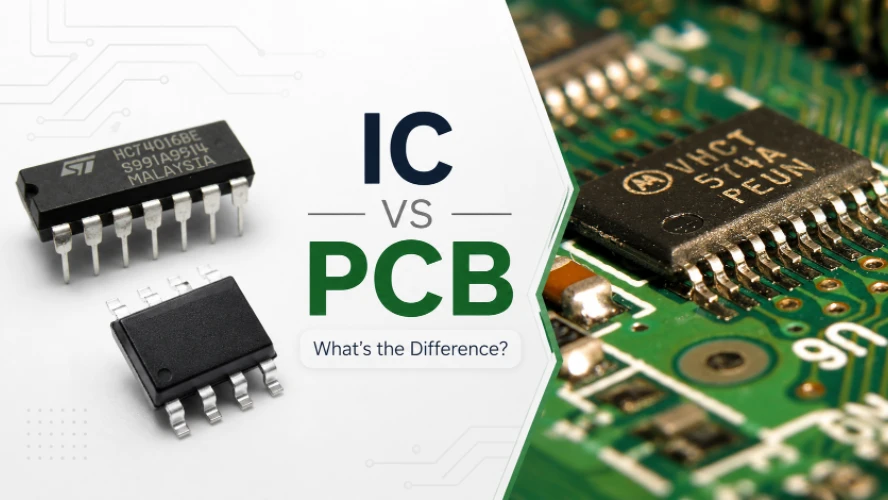
IC vs PCB: What’s the Difference and How They Work Together
Figure 1. IC vs PCB comparison showing the chip and the...

Electronic Reverse Engineering Service
You send us a physical PCB — or an electronic product...

High Frequency PCB Manufacturer China Selection Guide
Table of Contents China's HF PCB Manufacturing Capability...

Fast Turnaround Ceramic PCB Manufacturing
Table of Contents Why Most Turnaround Delays Originate on...
How to get a quote for PCBs
Let‘s run DFM/DFA analysis for you and get back to you with a report. You can upload your files securely through our website. We require the following information in order to give you a quote:
-
- Gerber, ODB++, or .pcb, spec.
- BOM list if you require assembly
- Quantity
- Turn time
For PCBA services, please provide your BOM (Bill of Materials) and any specific assembly instructions. We also offer DFM/DFA analysis to optimize your designs for manufacturability and assembly, ensuring a smooth production process.