
Electronic Reverse Engineering Service

You send us a physical PCB — or an electronic product containing PCBs. Our electronic reverse engineering service converts it into a complete, verified manufacturing package: Gerber files, schematic diagram, Bill of Materials, netlist, pick-and-place data, and assembly drawing. The goal is not documentation alone — it is a production-ready output your manufacturing team can use immediately to fabricate and assemble working boards, with no guesswork and fully controlled risk. This page explains our workflow, deliverables, cost structure, and the selection criteria that separate a reliable electronic reverse engineering partner from a risky one.
- What This Electronic Reverse Engineering Service Produces
- When Electronic Reverse Engineering Is the Right Decision
- Our Electronic Reverse Engineering Workflow — Phase by Phase
- Deliverables: Complete Manufacturing File Package
- Cost, Timeline, and How to Scope a Quote Accurately
- How to Evaluate an Electronic Reverse Engineering Manufacturer
- Highleap Electronics: Reverse Engineering + Fabrication + Assembly
1. What This Electronic Reverse Engineering Service Produces
A Manufacturing Outcome, Not Just a File Set
Many electronic reverse engineering engagements fail not because of poor scanning or weak component identification — they fail because the output cannot be sent to a factory without further engineering work. A board image and a “best-guess BOM” may look complete, but production exposes the real gaps: missing nets, wrong component footprints, incorrect passive values, unresolved inner layers, or obsolete parts with no qualified substitutes. Our service is built around one test: can the files we deliver be used to fabricate and assemble a working board at first attempt?
Three outcomes define a successful electronic reverse engineering project:
- Fabrication-ready Gerber data — verified against real manufacturing constraints on our own multilayer PCB manufacturing line, not just drawn to look correct.
- Assembly-ready package — BOM, pick-and-place file, and assembly drawing validated to produce consistent first-pass assembly yield across any qualified EMS facility.
- Functional prototype validation — boards built from the reconstructed package and electrically tested against original behavior before the project closes, so errors are found and corrected at prototype cost, not production cost.
Engineering Capability Summary
| Parameter | Specification |
|---|---|
| Layer count — non-destructive capture | Up to 20 layers via CT scanning; beyond 20 via controlled layer removal |
| CT scanning voxel resolution | 25 µm — resolves blind/buried vias, stacked vias, 0.4 mm pitch BGA pads |
| X-ray imaging resolution | 50 µm — standard multilayer and through-hole BGA inspection |
| Optical imaging system | 800–1200 DPI calibrated scan; Keyence VHX-7000 digital microscope for fine-pitch markings |
| Passive component measurement | LCR meter ±0.1% accuracy — identifies E24/E96 series values reliably |
| Board outline measurement | Digital calipers ±0.05 mm; CMM for critical connector and mounting geometry |
| CAD output formats | Altium Designer, KiCad, OrCAD, Cadence Allegro, Eagle — customer specifies |
| Board technology handled | Rigid FR4, HDI multilayer, rigid-flex, flex, metal core, ceramic substrate |
What a Professional Engagement Covers
Electronic reverse engineering is a controlled engineering process — inspection, measurement, reconstruction, and verification — not a scanning service. A complete engagement covers: physical board intake and risk mapping → schematic extraction from actual connectivity → Gerber layout reconstruction from layer capture → BOM generation with current-production sourcing → netlist extraction and layout-vs-schematic verification → prototype fabrication and functional validation. Each phase has defined acceptance criteria before the next begins.
2. When Electronic Reverse Engineering Is the Right Decision
High-Value Scenarios Where This Service Is the Correct Solution
- No design data exists: Original Gerbers, schematics, or BOM are lost, inaccessible, or held by a supplier who is unresponsive, dissolved, or unwilling to release files. Electronic reverse engineering is the only engineering path that recreates these files from the physical board.
- Legacy equipment that must stay operational: Replacement boards cannot be purchased; OEM support has ended; the equipment itself is too critical or costly to replace. Industrial machinery, process control systems, power electronics, and medical equipment are the most common scenarios. The goal is not just documentation — it is a reproducible supply of working replacement boards.
- Second-source and supply chain independence: You have a working product, but dependence on a single PCB supplier creates unacceptable delivery or continuity risk. A verified file package from electronic reverse engineering enables multi-source manufacturing from any qualified factory.
- Obsolete component substitution: Critical components on the board are end-of-life. The redesign work — identifying substitutes, verifying functional equivalence, updating the BOM and layout — is part of a complete electronic reverse engineering engagement, not a separate project.
- Manufacturing transfer to a new factory: You have hardware but no transferable design files. Electronic reverse engineering produces the complete, clean file set the new manufacturer needs — including DFM-reviewed Gerbers, fully specified BOM, and test documentation.
Representative Project Types
- Industrial motor drive controller (8-layer, 320 components): Original manufacturer had closed; customer needed 200 field-service replacement boards annually. CT scanning captured all inner layers; 18 obsolete components substituted with qualified current-production alternatives; prototype functional testing confirmed full behavioral equivalence. Full cycle from board receipt to tested prototype: 7 weeks.
- Power conversion module for process automation (6-layer, 240 components): Design files lost in a data center migration. Schematic extraction, layout reconstruction, and complete BOM generated. Prototype build validated against original switching behavior and thermal profile before file handoff to customer’s internal engineering team.
- Telecoms line card (12-layer HDI, 680 components, 0.5 mm pitch BGA): Second-source program to reduce single-supplier risk. CT scanning at 25 µm voxel size resolved all blind and buried vias; full Gerber, netlist, and assembly data generated; prototype build confirmed first-pass functionality. Customer qualified the package at a second factory within 9 weeks of project start.
When This Service Is Not the Best Path
- The original manufacturer can still supply the board or license the design — purchasing is faster and cheaper than reconstruction.
- The board is very simple (1–2 layers, fewer than 30 passives, no ICs) — your internal team may recreate it directly from visual inspection.
- The product’s function depends entirely on custom silicon with encrypted or permanently locked logic — the PCB layout can be reproduced, but functional equivalence cannot be guaranteed without the original code or a fully redesigned alternative.
Legal Authorization and Confidentiality Policy
- Authorized hardware only. We work exclusively on boards and products you own or are explicitly authorized to analyze — by ownership, purchase, contract, or written permission. We do not accept projects designed to infringe valid third-party intellectual property rights.
- NDA before any sample is received. We execute a confidentiality agreement before you ship your board. All photographs, measurements, and reconstructed files are treated as confidential project assets under controlled-access handling.
- File ownership. In standard manufacturing engagements, you receive the reconstructed outputs for your own internal production, maintenance, and sourcing use. Specific usage, transfer, and redistribution rights are defined in the project agreement before work begins.

3. Our Electronic Reverse Engineering Workflow — Phase by Phase
The quality difference between electronic reverse engineering providers is not in how they describe their process — it is in how accurately they capture inner layers, how rigorously they verify the reconstruction, and how closely the output is tested against actual manufacturing and assembly requirements. Below is the exact workflow we use on every project.
Phase 1 — Board Intake, Measurement, and Risk Mapping
- High-resolution imaging: Both sides photographed at 800–1200 DPI. All component markings, date codes, lot codes, and reference designators recorded. The Keyence VHX-7000 digital microscope is used for fine-pitch packages and abraded or obscured markings.
- Dimensional measurement: Board outline, mounting holes, connector positions, and keep-out zones measured with digital calipers at ±0.05 mm accuracy. Critical geometry — connector interfaces, guide-pin positions, card-edge fingers — verified with coordinate measurement equipment.
- Layer count determination: Edge inspection under magnification. For ambiguous boards, X-ray (50 µm) or CT scan (25 µm) is performed before committing to a capture method and work scope.
- Condition assessment: Damage, visible rework, conformal coating, encapsulation, added components, and cut traces are documented. Each factor affects capture accuracy and is disclosed explicitly at quote stage — no surprises mid-project.
- Written risk map: A document covering reconstruction risk by circuit area, recommended capture method per layer type, and any components flagged for functional testing rather than marking-based identification — delivered to the customer for review before Phase 2 begins.
Phase 2 — Component Removal and Identification
- Active components: All part markings recorded; datasheets sourced for pinout, package, and function. Obscured or abraded markings handled by functional testing or curve tracing. Every active component identified before BOM generation.
- Passive components: Values measured with LCR meter at ±0.1% accuracy. Package sizes physically measured. Tolerance estimated from measured values against E24/E96 standard series. Non-standard values flagged for engineering review.
- Connectors and mechanical parts: Manufacturer and part number identified; pin count, pitch, and mating connector confirmed. This is critical for accurate pick-and-place generation — wrong connector orientation is one of the most common assembly failures on reconstructed boards.
- Unmarked or custom components: Functional testing, curve tracing, and controlled decapsulation determine component type and parameters where marking identification is not possible. Every unidentified component is documented with its confidence level in the BOM — no component is left as “unknown.”
Output: the initial Bill of Materials — component-by-component with values or part numbers, package sizes, reference designators, current-production sourcing options, and recommended substitutions for any end-of-life parts identified.
Phase 3 — Board Imaging and Inner Layer Capture
Inner layer capture accuracy determines whether the reconstructed Gerber package is manufacturable or not. This is the phase where the difference between a usable file set and a failed project is made.
- Outer layers: Calibrated optical scanning captures copper patterns, solder mask openings, and silkscreen with full dimensional fidelity.
- Inner layers — standard multilayer (4–8 layers, no HDI): X-ray imaging at 50 µm resolution. Non-destructive. Suitable for boards without blind or buried vias.
- Inner layers — HDI and complex multilayer: CT scanning at 25 µm voxel size. Non-destructive. Simultaneously reconstructs all layers in 3D, resolving blind vias, buried vias, stacked vias, and via-in-pad structures that X-ray cannot differentiate. Required for any board with HDI construction. As documented in the technical literature on PCB reverse engineering, CT scanning is now the established standard for non-destructive inner layer capture on complex multilayer boards.
- Inner layers — when imaging cannot resolve features: Controlled layer removal. Sequential sanding and etching exposes each copper layer for direct optical imaging. Destructive — the board sample is consumed. Recommended when multiple samples are available, so non-destructive verification can proceed on remaining boards in parallel.
Phase 4 — Digital Layout Reconstruction
- All copper traces recreated to match position, width, and layer assignment from imaging data — not estimated or interpolated.
- Via types (through-hole, blind, buried, microvia, via-in-pad) identified and placed at correct coordinates with correct drill dimensions.
- Component footprints created from measured pad positions and IPC standard package dimensions, then placed at recorded X/Y coordinates and orientation.
- Board outline, mounting holes, slots, and keep-out zones rebuilt from physical measurements taken in Phase 1.
Output: Gerber files in RS-274X and Gerber X2 format, plus Excellon drill files — the complete fabrication data set required to manufacture the board at any qualified PCB factory.
Phase 5 — Schematic Reconstruction
- Functional block mapping: Power supply, processor/control, analog signal chains, communication interfaces, and protection circuits identified and mapped as logical blocks before detailed net tracing begins.
- Net tracing and topology analysis: Each net traced from layout to schematic with circuit function identified (switching regulator, differential amplifier, UART interface, protection network). Reference designators assigned consistently with the BOM.
- Schematic drawing: Drawn in standard engineering format with meaningful net names, logical hierarchy, and clear reference designator mapping to layout and BOM. Schematics produced natively in Altium Designer, KiCad, OrCAD, or Cadence Allegro per the customer’s toolchain — so your engineering team can modify the design directly without a conversion step.
- Cross-verification against layout: Every net in the schematic independently verified against the physical board layout before delivery. Mismatches resolved before the file set is released.
Phase 6 — Netlist Extraction and Verification
- Layout-vs-schematic (LVS) check: Connectivity extracted from layout compared against schematic connectivity. Mismatches — missed traces, incorrectly interpreted junctions, net short/open — identified and corrected.
- Electrical rule check (ERC): Schematic validated for power pin connections, output-to-output conflicts, floating inputs, and reference designator consistency.
- Design rule check (DRC): Layout validated against manufacturing minimums — trace width, spacing, via clearances, annular ring, pad sizes — so the Gerbers comply with IPC-2221 design rules and can be manufactured without CAM-stage rejections.
Phase 7 — Prototype Fabrication and Functional Validation
This phase is what transforms a documentation set into a confirmed, manufacturable design. For any program where multi-year supply is the goal, prototype validation is the insurance policy that prevents expensive production failures.
- Prototype PCB fabrication from the reconstructed Gerbers and drill files, built on our own fabrication line under the same process controls used for production boards.
- Component assembly per the reconstructed BOM and pick-and-place file. Obsolete-part substitutes assembled alongside original-part versions where stock is available for direct comparison.
- Functional testing: Power-on sequencing, key signal node verification, communication interface testing, and behavioral comparison against the original board. Any discrepancy triggers root-cause analysis — typically a missed net, incorrect passive value, or footprint offset — followed by correction and re-verification.
- Test report: Documented test results, discrepancies found, and corrections applied. Included in the final deliverable package as validation evidence for your engineering signoff.
4. Deliverables: Complete Manufacturing File Package
Standard Deliverables
| Deliverable | Format | Used For |
|---|---|---|
| Schematic diagram | PDF + native CAD (Altium, KiCad, OrCAD, Allegro) | Circuit understanding, troubleshooting, future modification |
| Gerber files — all layers | RS-274X / Gerber X2 | PCB fabrication at any qualified factory |
| Drill files | Excellon — plated and non-plated separated | PCB fabrication — mechanical and laser drilling |
| Bill of Materials | Excel / CSV — manufacturer P/N, alternates, sourcing notes per component | Component procurement; obsolete part substitution |
| Netlist | IPC-D-356 + native CAD format | Electrical test fixture generation; design verification |
| Pick-and-place file | CSV — X/Y, rotation, layer, reference designator | SMT automated assembly; first-article inspection |
| Assembly drawing | PDF — top and bottom views, component outlines, reference designators | Manual assembly reference; quality inspection |
| Prototype test report | PDF — test procedure, pass/fail results, discrepancies, corrections | Validation evidence; engineering and quality signoff |
Optional Additions
- 3D board model: STEP file with component bodies for mechanical integration verification and enclosure clearance checking.
- Obsolete component substitution report: For each EOL component, documented alternative part numbers with specification comparison table and any assembly or qualification notes for the substitute.
- Fabricated and tested prototype boards: Some programs include a full validation build — tested, functional boards delivered alongside the documentation package, ready for customer-side system integration testing.
- Production-lot manufacturing: Following a validated prototype, full production volume fabricated and assembled in-house under the same quality controls. No separate factory qualification step — the same facility that validated the design builds the production run.
Request Electronic Reverse Engineering Quote
5. Cost, Timeline, and How to Scope a Quote Accurately
Cost and Timeline by Complexity
| Factor | Low Complexity | Medium Complexity | High Complexity |
|---|---|---|---|
| Layer count | 1–2 layers | 4–6 layers | 8–20+ layers, HDI |
| Component count | 20–100 | 100–500 | 500–2,000+ |
| Board area | Under 100 cm² | 100–400 cm² | Over 400 cm² |
| Unmarked / custom components | None | 1–5 | 5+, including custom ASICs |
| Indicative cost range | $3,000–$5,000 | $5,000–$15,000 | $15,000–$50,000+ |
| Typical timeline | 2–3 weeks | 3–6 weeks | 6–12 weeks |
These ranges are indicative. Final pricing is confirmed after reviewing board photographs and specifications. When comparing proposals from multiple providers, confirm what each quote explicitly includes and excludes on these four scope variables:
- Inner layer capture method: X-ray, CT scanning, or destructive layer removal? The cost and accuracy differ significantly. CT scanning for complex multilayer and HDI boards adds cost but is the only non-destructive method that reliably resolves all layer types simultaneously.
- Prototype fabrication, assembly, and functional testing: Many providers quote file delivery only. A quote that includes a validation build eliminates the risk of discovering file errors at production volume.
- Obsolete component substitution validation: Identifying an alternative part is different from verifying it performs identically in circuit. Substitution validation should be part of the prototype test scope, not left to the customer to discover.
- Sample quantity and board condition: More samples allow non-destructive capture in parallel with backup destructive verification. Conformal-coated, encapsulated, or damaged boards increase effort and may extend timelines — these factors should be disclosed in the quote, not discovered mid-project.
The Main Drivers of Higher Cost
- Layer count: Each additional layer requires separate imaging, reconstruction, and cross-verification. Complexity scales faster than layer count — an 8-layer board carries approximately 6–8× the engineering effort of a 2-layer board, not 4×, due to inter-layer connectivity complexity.
- HDI construction: Microvias, blind/buried vias, and fine-pitch BGA arrays require CT scanning rather than X-ray. Via-in-pad and stacked-via structures need additional verification steps beyond standard layer tracing.
- Unmarked or custom components: Each unidentifiable component requires functional testing, curve tracing, or physical analysis — adding hours to days of engineering time per component, not counted in the basic pricing model.
- Board damage: Burnt traces, corroded pads, or physically missing sections require engineering inference — reconstructing missing portions from surrounding circuit topology rather than direct observation. This is higher-risk work and is priced accordingly.
Information Required for an Accurate Quote
- Photographs of both board sides — close enough to read component markings
- Board dimensions and visible layer count estimate (edge inspection if accessible)
- Known information about board function, operating environment, or system context
- Specific deliverables required: schematic only, full Gerber package, prototype boards, production-lot manufacturing, or combination
- Number of sample boards available for analysis
- Whether conformal coating, encapsulation, or visible physical damage is present
6. How to Evaluate an Electronic Reverse Engineering Manufacturer
Technical Capability Checklist
- ☑ All three inner-layer capture methods available in-house: high-resolution optical scanning, X-ray, and CT scanning — not just one or two
- ☑ Demonstrated experience with your specific board technology: standard multilayer FR4, HDI with blind/buried vias, rigid-flex, ceramic, fine-pitch BGA
- ☑ Multi-platform CAD output: Altium, KiCad, OrCAD, Cadence Allegro — not locked to a single tool that forces you into a format conversion
- ☑ In-house PCB fabrication capability — so the reconstructed Gerbers are verified against real manufacturing constraints, not just reviewed on screen
- ☑ In-house PCB assembly capability — so the BOM and pick-and-place files are validated through actual assembly, not visual review alone
- ☑ Component identification and obsolete component sourcing capability — including cross-reference databases and functional substitution testing, not just Google searches
Quality and Process Indicators
- ☑ NDA executed before any board or file is received — your design is your intellectual property from the moment you hand it over, not after a contract is signed weeks later
- ☑ ISO 9001 certified quality management — documented and auditable processes, not ad hoc engineering
- ☑ Full project scope quoted upfront, in writing — no mid-project additions for “complex analysis” that should have been anticipated in the initial assessment
- ☑ Files delivered in fully standard, usable formats regardless of whether you use the provider’s fabrication — any provider who embeds deliberate errors to force you into their factory is disqualifying themselves, not demonstrating capability
- ☑ Prototype validation included or available as a priced option — verified by building and electrically testing a board, not by visual inspection of the Gerber file
Red Flags That Should Disqualify a Provider
- ⚠ Quote dramatically lower than all competitors — usually means scope exclusions (no CT scanning, no prototype validation) that add cost later, or lower capture quality that reveals itself at production
- ⚠ No prototype validation offered at any price — the only way to know a reconstructed file package is correct is to build a board and test it
- ⚠ Refusal to deliver Gerber, ODB++, or native CAD files in standard format — file-locking is a commercial tactic that has no technical justification
- ⚠ No NDA process — your board’s design information is exposed from the moment it arrives
- ⚠ No in-house PCB fabrication — a provider who cannot build the board they reconstruct cannot know whether their Gerbers will work in production
7. Highleap Electronics: Reverse Engineering + PCB Fabrication + Assembly
Highleap Electronics is a PCB manufacturing and assembly factory. For electronic reverse engineering, this matters because the reconstructed files are not just drawn to look correct — they are verified on the same fabrication and assembly equipment that will build the production boards. A provider who cannot manufacture what they reverse engineer cannot give you meaningful assurance that their files will work.
What an End-to-End Engagement Includes
- Complete electronic reverse engineering: Board analysis → component identification → schematic extraction → Gerber layout reconstruction → BOM generation → netlist extraction and LVS verification → functional prototype validation
- Integrated PCB fabrication: Prototype and production boards built in-house on our multilayer PCB manufacturing line — up to 60 layers, HDI, rigid-flex, high-frequency substrate materials. No delay for factory qualification — the same facility that reconstructed the design builds the board.
- Integrated PCB assembly: SMT and through-hole assembly in-house using the reconstructed BOM and pick-and-place data. Full assembly services including AOI, X-ray inspection, and functional testing on every prototype validation build.
- Transparent scope and pricing: Full project cost quoted upfront, defined in writing. No mid-project additions. Files delivered in fully usable standard formats — they will work at any qualified factory, not only ours. You are never locked in.
- NDA protection: Standard Non-Disclosure Agreement executed before your board arrives — not after.
Quality Certifications
- ISO 9001:2015 — documented quality management system across all fabrication and assembly processes
- IATF 16949 — automotive-grade process discipline, applied to reverse engineering programs requiring the highest level of documentation and change control
- IPC-A-600 and IPC-A-610 Class 2 and Class 3 acceptance criteria — applied to prototype validation builds and any production boards shipped under the reconstructed file package
- Comprehensive board testing — AOI, X-ray, in-circuit test, and functional verification on every prototype validation build
Frequently Asked Questions
What board technologies can you reverse engineer?
Standard rigid FR4 (1–60+ layers), HDI with blind and buried vias, rigid-flex, flex, metal-core, and ceramic substrate boards. We handle both simple 2-layer power supplies and complex 16-layer telecom line cards with dense BGA arrays.
Can you handle boards with conformal coating or physical damage?
Yes, with qualification. Conformal coating is removed chemically or mechanically before analysis. Damaged boards — burnt traces, corroded pads, missing sections — are handled with circuit-topology inference documented explicitly in the reconstruction, with confidence level noted per affected area. No damaged area is left undisclosed in the deliverable package.
Do your files work at other manufacturers, not just Highleap?
Yes, without restriction. We deliver RS-274X Gerber, Excellon drill, IPC-D-356 netlist, and native CAD files compatible with any qualified PCB factory and EMS provider. There are no embedded restrictions, watermarks, or deliberate errors. You are not obligated to use our fabrication service after receiving the files.
What happens if the prototype does not match the original board’s behavior?
We investigate, correct, and re-verify before the project closes. Prototype discrepancies are part of the validation process — they are why prototype testing exists. The test report documents what was found and what was corrected, so the final file package reflects a confirmed, functional design.
How do I start?
Send clear photographs of both board sides through our quote portal. We review within one business day and return a detailed scope proposal: capture method, deliverables, timeline, and complete pricing. For complex or high-value boards, a preliminary NDA-protected consultation is available before you commit to shipping any hardware.
Sabrina has over 18 years of experience in the PCB industry, with a strong background in CAM engineering and PCB file review. She supports PCB projects from prototype to volume production, focusing on manufacturability and process reliability. Her work helps engineering teams reduce production risk and achieve stable, high-quality PCB manufacturing results.

Recommended Posts
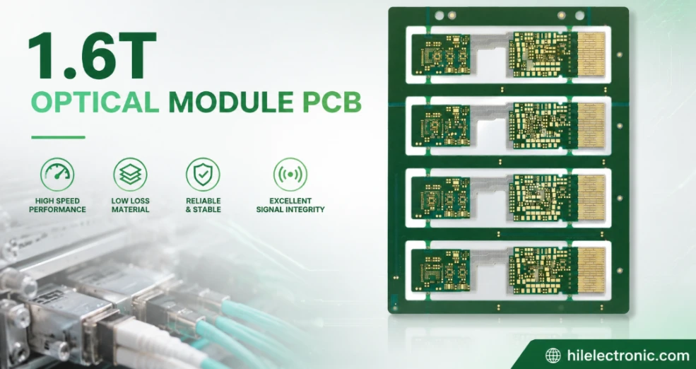
1.6T Optical Module PCB Manufacturing and Assembly Service
Table of contents1.6T Module Architectures and PCB...
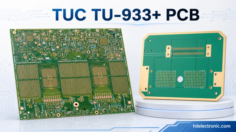
TUC TU-933+ PCB Manufacturing for Super-Low-Loss High-Speed Systems
Table of contentsWhat Is TU-933+ PCB Material?Why TU-933+...
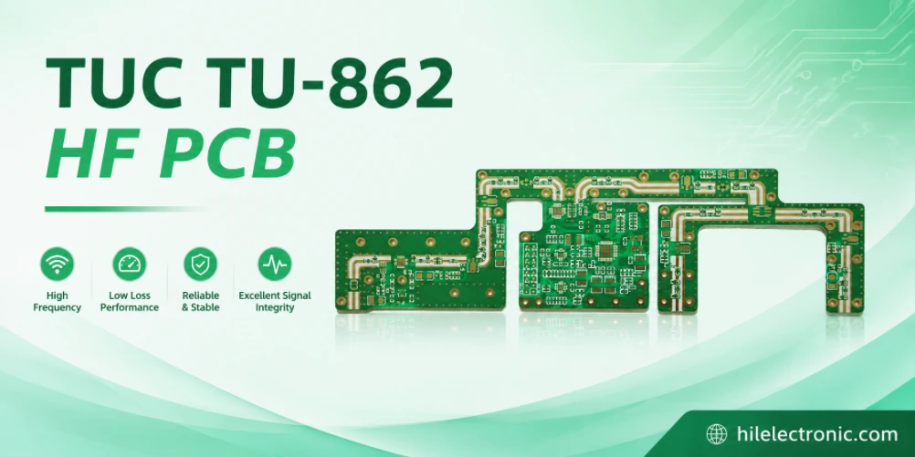
TUC TU-862 HF PCB Manufacturing and Assembly Service
Table of contentsWhat Is TU-862 HF?Why Choose TU-862 HF...
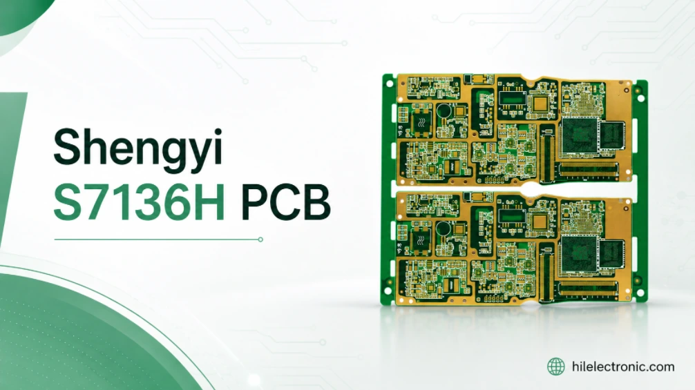
Shengyi S7136H PCB Manufacturing and Assembly Service
Table of contentsWhat Is a Shengyi S7136H PCB?Why...
How to get a quote for PCBs
Let us run DFM/DFA analysis for you and get back to you with a report.
You can upload your files securely through our website.
We require the following information in order to give you a quote:
-
- Gerber, ODB++, or .pcb, spec.
- BOM list if you require assembly
- Quantity
- Turn time
In addition to PCB manufacturing, we offer a comprehensive range of electronic services, including PCB design, PCBA (Printed Circuit Board Assembly), and turnkey solutions. Whether you need help with prototyping, design verification, component sourcing, or mass production, we provide end-to-end support to ensure your project’s success. For PCBA services, please provide your BOM (Bill of Materials) and any specific assembly instructions. We also offer DFM/DFA analysis to optimize your designs for manufacturability and assembly, ensuring a smooth production process.