
HDI PCB Manufacturing Services in China | Cost-Optimized

This article delves into the sophisticated aspects of HDI PCB Manufacturing, highlighting our advanced capabilities, material expertise, and stringent quality assurance processes that establish us as a trusted partner for high-performance PCB solutions.
Advanced HDI PCB Manufacturing Capabilities
Highleap Electronic is equipped with the latest technologies and expertise to deliver HDI PCBs that meet the highest industry standards. Our comprehensive capabilities include:
| Feature | Capability |
|---|---|
| Max Layer | 60 Layers |
| Inner Layer Min Trace/Space | 2 mil / 2 mil |
| Out Layer Min Trace/Space | 2 mil / 2 mil |
| Inner Layer Max Copper | 10 oz |
| Out Layer Max Copper | 10 oz |
| Min Mechanical Drilling/Annular Ring | 0.15 mm / 0.127 mm |
| Min Laser Drilling/Annular Ring | 0.075 mm / 0.075 mm |
| Aspect Ratio (Mechanical Drilling) | 20:1 |
| Aspect Ratio (Laser Drilling) | 1:1 |
| Press Fit Hole Tolerance | ±0.05 mm |
| PTH Tolerance | ±0.075 mm |
| NPTH Tolerance | ±0.05 mm |
| Countersink Tolerance | ±0.15 mm |
| Board Thickness | 0.4 mm – 8 mm |
| Board Thickness Tolerance | <1.0 mm: ±0.1 mm >=1.0 mm: ±10% |
| Impedance Tolerance | Single-Ended: ±5Ω (≤50Ω), ±7% (>50Ω) Differential: ±5Ω (≤50Ω), ±7% (>50Ω) |
| Min Board Size | 10 mm x 10 mm |
| Max Board Size | 22.5 inches x 30 inches |
| Contour Tolerance | ±0.1 mm |
| Min BGA | 7 mil |
| Min SMT | 7 x 10 mil |
| Surface Treatment |
ENIG, Gold Finger, Immersion Silver, Immersion Tin, HASL, OSP, ENEPIG, Flash Gold, Hard Gold Plating |
| Solder Mask | Green, Black, Blue, Red, Matt Green |
| Min Solder Mask Clearance | 1.5 mil |
| Min Solder Mask Dam | 3 mil |
| Legend | White, Black, Red, Yellow |
| Min Legend Width/Height | 4 mil / 23 mil |
| Strain Fillet Width | / |
| Bow & Twist | 0.3% |
Comprehensive HDI PCB Capabilities
Highleap Electronic is capable of manufacturing HDI PCBs with the following specifications:
- Layer Configurations: 4 to 60 layers, supporting complex via structures such as 1+N+1, 2+N+2, and 3+N+3 configurations with blind, buried, and stacked vias.
- Material Flexibility: Supports a variety of substrates including FR4 (standard and high Tg), Rogers, Arlon, and polyimide-based laminates for rigid-flex applications.
- Dimension and Thickness Variability: Capable of manufacturing boards ranging from 10 mm x 10 mm to 22.5 inches x 30 inches, with thicknesses from 0.4 mm to 8 mm.
- Copper Weight: Offers copper thickness options from 0.5 oz to 10 oz (finished), suitable for high-current applications and thermal management.
- Advanced Features: Includes cavity PCB processes, via-in-pad with conductive or non-conductive fills, buried capacitors for prototype PCBs, and flex-rigid combinations for versatile design requirements.
- Surface Treatments: ENIG, Gold Finger, Immersion Silver, Immersion Tin, HASL, OSP, ENEPIG, Flash Gold, Hard Gold Plating.
- Minimum Requirements:
- Min BGA: 7 mil
- Min SMT: 7 x 10 mil
- Min Solder Mask Clearance: 1.5 mil
- Min Solder Mask Dam: 3 mil
- Min Legend Width/Height: 4 mil / 23 mil
- Additional Capabilities:
- Press Fit Hole Tolerance: ±0.05 mm
- Countersink Tolerance: ±0.15 mm
- Strain Fillet Width: /
- Bow & Twist: 0.3%
Why Choose Highleap Electronic as Your HDI PCB Manufacturer?
At Highleap Electronic, we pride ourselves on being more than just a manufacturer—we are your trusted HDI PCB manufacturer and strategic partner in high-density PCB design and production. Here’s why leading companies trust us for their high-density PCB requirements:
1. Unparalleled Manufacturing Capabilities
We push the boundaries of HDI PCB technology with the following capabilities:
- Max Layer Count: Up to 60 layers for highly complex designs.
- Min Trace/Space: As low as 2/2 mil for both inner and outer layers.
- Copper Weight: Up to 10 oz for superior thermal and current-carrying capacity.
- Drilling Precision: Mechanical drilling with a minimum size of 0.15 mm and laser drilling down to 0.075 mm.
- Aspect Ratios: 20:1 for mechanical drilling and 1:1 for laser drilling.
- Board Thickness: Ranges from 0.4 mm to 8 mm, with thickness tolerances of ±0.1 mm for boards below 1.0 mm and ±10% for thicker boards.
- Impedance Control: Precision-controlled single-ended and differential impedance tolerances of ±5Ω (≤50Ω) and ±7% (>50Ω).
- Surface Finishes: ENIG, ENEPIG, Immersion Silver, Immersion Tin, HASL, OSP, and more.
These advanced capabilities position Highleap Electronic as a top-tier HDI PCB manufacturer for complex, high-reliability applications.
2. Tailored Solutions for Unique Requirements
If you’re struggling to find an HDI PCB manufacturer that meets your exact specifications, Highleap Electronic’s team of expert process engineers is ready to help. We work closely with you to create tailored HDI solutions that ensure manufacturability, reliability, and performance. Whether it’s a highly customized material stack-up or intricate via configurations, we make your ideas a reality.
3. Comprehensive Quality Control
We implement rigorous testing at every step of the manufacturing process, including:
- Automated Optical Inspection (AOI): Identifies even the smallest defects in traces, solder masks, and vias.
- X-ray Inspection: Ensures the structural integrity of blind and buried vias and complex solder joints.
- Electrical Testing: Verifies impedance, continuity, and signal integrity for reliable performance.
- Functional Testing: Simulates real-world conditions to validate performance before shipment.
4. Fast Turnaround Times
With advanced production workflows and an efficient team, we provide fast turnaround times, even for complex designs. Whether you need a prototype or a full production run, we deliver on time without compromising quality.
As a seasoned HDI PCB manufacturer, Highleap Electronic combines precision engineering, flexible production, and world-class quality assurance to support your most demanding projects.
HDI PCB Design Considerations for Seamless Manufacturing
To achieve superior results in HDI PCB manufacturing, partnering with an experienced HDI PCB manufacturer who understands design best practices is essential.
Impedance matching is a critical factor in ensuring signal integrity, particularly for high-speed and RF applications. Accurate impedance control reduces signal loss and enhances performance. Thermal management is another key consideration; incorporating thermal vias and selecting materials with efficient heat dissipation properties are necessary to prevent overheating in high-density circuits.
Effective microvia design is fundamental in HDI PCB manufacturing. Choosing the right HDI PCB manufacturer ensures proper implementation of via-in-pad configurations and staggered or stacked microvias, which allows for increased layer interconnectivity, higher density, and minimal signal interference. These techniques enable reliable and efficient performance in the compact layouts demanded by modern electronics.
Material selection plays a crucial role in optimizing the performance and manufacturability of HDI PCBs. Advanced materials such as Rogers, Arlon, or high-Tg FR4 provide the necessary electrical stability and thermal durability for complex designs.
At Highleap Electronic, a leading HDI PCB manufacturer, our team of expert engineers works closely with clients to refine designs and align them with manufacturing best practices. This ensures seamless production and the highest quality outcomes in every HDI PCB project.

How We Help Reduce Costs in Your HDI PCB Manufacturing
At Highleap Electronic, we focus on providing cost-efficient solutions in HDI PCB Manufacturing without compromising on quality or performance. Through design optimization, advanced manufacturing techniques, and efficient material utilization, we help our clients achieve significant cost savings while maintaining high standards.
1. Design Optimization for Cost Efficiency
Our expert engineering team collaborates with you to refine your HDI PCB design for manufacturability. By reducing unnecessary complexity, such as overly dense layer stack-ups or redundant via configurations, we streamline production processes.
Utilizing staggered or stacked microvias strategically can further enhance layer connectivity while lowering production costs. We also focus on optimizing trace layouts to minimize the use of copper and other materials, ensuring your design remains functional and cost-effective.
2. Optimized Panelization to Maximize Material Utilization
One of the most effective ways to reduce costs in HDI PCB Manufacturing is by optimizing panelization. Our engineering team uses advanced software tools to design the most efficient panel layouts, ensuring the highest possible material utilization. By strategically arranging PCB designs on a panel, we reduce material waste and increase production yields. This not only minimizes raw material costs but also decreases the overall manufacturing time.
Additionally, by combining different designs (multi-project panelization) or arranging boards with minimal clearance, we can further maximize material usage. This approach is particularly beneficial for small-batch or prototype runs, where cost efficiency is often a challenge.
3. Strategic Material Selection and Usage
Material selection is a critical factor in balancing performance and cost. We guide you in choosing high-quality yet cost-effective materials, such as hybrid laminates that combine FR4 with advanced materials like Rogers for applications requiring specific electrical properties. By selecting materials tailored to your product’s requirements, we reduce unnecessary expenses while ensuring optimal functionality.
Efficient use of materials, such as utilizing thinner copper cladding where possible or selecting high-Tg FR4 for applications that don’t require ultra-high performance, further contributes to cost savings. Our team also ensures minimal waste during the manufacturing process, maximizing the yield from each sheet of laminate.
4. Advanced Manufacturing Techniques to Improve Efficiency
Highleap Electronic employs cutting-edge manufacturing technologies to reduce production costs. High-precision laser drilling and automated processes ensure high yields with minimal defects. This efficiency directly translates into reduced rework and waste, helping to keep costs low.
For example:
- Fine Trace Optimization: Our ability to produce traces as fine as 2 mil ensures more circuits can be placed within a smaller area, reducing the number of layers required.
- Efficient Surface Finishes: Offering surface treatments such as ENIG, OSP, and HASL in combination with your design needs helps reduce unnecessary costs while ensuring reliability.
5. Streamlining Supply Chain and Production
Our streamlined production workflows and strong supplier relationships enable us to source materials cost-effectively and meet deadlines efficiently. Combining this with in-house capabilities, such as PCB assembly and prototyping, reduces lead times and additional costs related to outsourcing.
Tailored Cost-Reduction Strategies
At Highleap Electronic, we tailor every project to balance cost and quality. Whether it’s through design refinement, material selection, optimized panelization, or advanced manufacturing techniques, our team is committed to helping you maximize the value of your investment.
Contact us today to discuss how we can lower your HDI PCB manufacturing costs while delivering reliable, high-performance products. With Highleap Electronic, cost-efficiency and excellence go hand in hand.
Conclusion
High-Density Interconnect (HDI) PCB Manufacturing is a critical enabler of modern electronic innovation, offering unparalleled circuit density, enhanced electrical performance, and design flexibility.
At Highleap Electronic, our advanced manufacturing capabilities, comprehensive HDI PCB material expertise, and stringent quality assurance processes position us as a leading HDI PCB manufacturer in the market. By partnering with us, businesses can harness the full potential of HDI technology to develop cutting-edge electronic products that meet the highest standards of performance and reliability.
Embrace the future of electronics with Highleap Electronic’s HDI PCB manufacturing, assembly, and comprehensive services. Contact us today to discuss how our expertise as an experienced HDI PCB manufacturer can elevate your next project, ensuring your products excel in the competitive and rapidly evolving electronics landscape.
Contact Highleap Electronic Today
If you haven’t found an HDI PCB manufacturer that can meet your specific needs, welcome to consult Highleap Electronic. Our outstanding team of process engineers can provide perfect production solutions tailored to your product, ensuring optimal manufacturability and performance.
Frequently Asked Questions (FAQ)
1. What Are the Key Differences Between Blind and Buried Vias?
Blind vias connect outer layers to one or more inner layers without penetrating the entire PCB, making them visible from one side. Buried vias are entirely internal, connecting only inner layers and remaining hidden from both sides of the PCB.
2. How Do Blind and Buried Vias Affect PCB Manufacturing Costs?
Blind and buried vias generally increase manufacturing costs due to the additional processing steps, such as multiple lamination cycles and precision drilling. However, the benefits in space optimization and performance often justify the higher costs for complex and high-density PCBs.
3. What Challenges Are Associated with Manufacturing Blind and Buried Vias?
Challenges include maintaining precise alignment during drilling and lamination, controlling copper thickness accurately, and managing resin-filled vias to prevent defects. Advanced equipment and strict adherence to CAM specifications are essential to overcome these challenges.
4. How Do Blind and Buried Vias Enhance PCB Reliability?
By reducing the length of electrical connections and minimizing the number of through-holes, blind and buried vias lower electrical resistance and improve signal integrity. This leads to more reliable performance, especially in high-speed and high-frequency applications.
5. Which Industries Benefit the Most from Blind and Buried Vias in PCBs?
Industries such as telecommunications, consumer electronics, aerospace, automotive, and medical devices benefit significantly. These sectors require high-density, compact, and reliable PCBs to support advanced functionalities and stringent performance standards.

Recommended Posts

Outdoor Lighting PCB Manufacturing & Assembly by Highleap Electronics
Figure 1. outdoor lighting PCB production and assembly...

Lighting PCB Manufacturer: PCB Fabrication, PCB Assembly & Turnkey LED Lighting
Figure 1. Lighting PCB manufacturer overview for LED light...

Audio DSP: How It Works, What It Does, and How the PCB Behind It Gets Built
On this page What Audio DSP Actually Does Core Audio DSP...
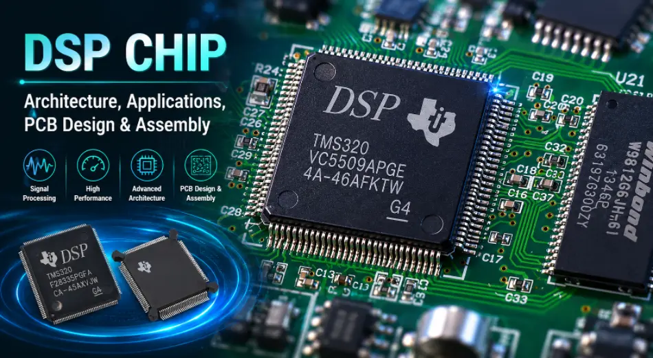
DSP Chip PCB Design and Assembly Guide
High-performance DSP chip boards need design, fabrication,...
How to get a quote for PCBs
Let us run DFM/DFA analysis for you and get back to you with a report.
You can upload your files securely through our website.
We require the following information in order to give you a quote:
-
- Gerber, ODB++, or .pcb, spec.
- BOM list if you require assembly
- Quantity
- Turn time
In addition to PCB manufacturing, we offer a comprehensive range of electronic services, including PCB design, PCBA (Printed Circuit Board Assembly), and turnkey solutions. Whether you need help with prototyping, design verification, component sourcing, or mass production, we provide end-to-end support to ensure your project’s success. For PCBA services, please provide your BOM (Bill of Materials) and any specific assembly instructions. We also offer DFM/DFA analysis to optimize your designs for manufacturability and assembly, ensuring a smooth production process.