
ENIG PCB Surface Finish for Fine-Pitch Assembly

Introduction
Electroless Nickel Immersion Gold (ENIG) is a dual-layer surface finish used in printed circuit boards (PCBs), featuring nickel as a barrier layer and gold as a protective layer. As the demands on PCB reliability and performance increase—especially in 5G, automotive, aerospace, and consumer electronics—ENIG has become a go-to finish. Its flat surface, excellent corrosion resistance, and solderability make it ideal for fine-pitch components, BGAs (Ball Grid Arrays), and HDI (High-Density Interconnect) designs. However, ENIG’s advantages are accompanied by several critical technical challenges.
This article provides in-depth technical insights into ENIG PCB technology, its benefits, manufacturing intricacies, and advanced applications, while addressing challenges such as black pad defects and process variations. We also compare ENIG with other surface finishes to help engineers and designers make informed decisions.
Core Manufacturing Process of ENIG PCBs
The ENIG process consists of precise chemical steps where each stage must be carefully controlled to ensure reliability. Below is a more technical breakdown of the key phases involved:
- Surface Preparation (Microetching):
The copper surface is cleaned, followed by microetching to create a rough profile that enhances the adhesion of the nickel layer. Even minute contamination or improper etching can lead to defects during later stages. - Electroless Nickel Deposition:
A nickel-phosphorous (Ni-P) alloy layer, typically 3–6 microns thick, is deposited using a chemical reaction. No external electrical current is used, ensuring a uniform layer even on non-planar surfaces. The phosphorus content influences the mechanical properties of the nickel.- High-phosphorus nickel (10–12%) enhances corrosion resistance, especially for medical devices and marine electronics.
- Low-phosphorus nickel (<5%) improves wear resistance, suitable for connectors and switches.
- Activation for Gold Deposition:
The nickel surface is chemically activated to prepare it for the gold plating step. Poor activation or contamination at this stage can result in partial gold coverage and soldering issues. - Immersion Gold Deposition:
Gold ions from the bath chemically replace nickel atoms on the surface, forming a thin immersion gold layer (0.05–0.1 microns thick). The gold acts as an anti-oxidation layer and maintains solderability during storage. Precise control is required, as insufficient gold coverage leads to oxidation of the nickel, causing failures.
ENIG and the Black Pad Defect: Causes and Mitigation
One of the most significant technical challenges with ENIG is black pad defect, a failure mode where excess phosphorus from the nickel layer migrates to the surface, forming nickel-phosphide crystals. This contamination inhibits wetting during soldering and results in brittle solder joints prone to cracks. Black pad defect is catastrophic in applications such as automotive control units and aerospace electronics where failure is not an option.
Causes of Black Pad Defect
- Overactive Gold Bath: An overly aggressive immersion gold bath can corrode the nickel, leaving excessive phosphorus on the surface.
- Improper Bath Chemistry Control: Variations in pH or temperature can lead to non-uniform deposition of nickel, increasing the risk of black pad defects.
- Excessive Gold Thickness: Over-plating gold can accelerate the leaching of nickel, resulting in black pad formation.
Mitigation Strategies
- Tighter Process Control: Implement automated monitoring of bath chemistry (pH, temperature) to maintain process consistency.
- Limit Gold Thickness: Keep the gold thickness below 0.1 microns to prevent over-aggressive nickel leaching.
- Periodic Inspections: Conduct cross-sectional analysis of ENIG coatings to detect early signs of phosphorus migration.
Thermal Cycling and Solder Joint Reliability in ENIG PCBs
ENIG PCBs are often exposed to thermal cycling during operation, particularly in automotive and aerospace applications. Each cycle induces thermal expansion and contraction in solder joints, stressing the material interfaces between the solder, gold, nickel, and copper. This thermal stress can result in:
- Intermetallic Layer Growth: The interface between the solder and the ENIG surface can develop nickel-tin (Ni-Sn) intermetallics, which are brittle and prone to fracture over time.
- Stress Cracking: Repeated thermal cycles can cause small cracks to form in solder joints, particularly around areas with thin gold layers or non-uniform nickel deposits.
Design Solutions to Improve Reliability
- Controlled Reflow Profiles: Proper temperature control during solder reflow minimizes stress at material interfaces.
- Thicker Nickel Layers: Increasing the nickel thickness helps reduce the formation of brittle intermetallic layers.
- Alternative Finishes (ENEPIG): For extreme reliability requirements, ENEPIG (Electroless Nickel Electroless Palladium Immersion Gold) is used to prevent intermetallic growth by adding a palladium barrier layer.
Comparison of ENIG with Other Surface Finishes
Choosing the right PCB surface finish is critical for achieving optimal performance, reliability, and cost efficiency. Each surface finish offers unique advantages and challenges, depending on the application, operating conditions, and budget constraints. Below is an in-depth technical comparison of ENIG and other commonly used surface finishes, including ENEPIG, HASL, OSP, Immersion Silver, and Immersion Tin.

Applications of ENIG PCB in High-Performance Systems
ENIG is indispensable in industries that require high reliability and precision. Below are some of its key applications:
5G Infrastructure and Consumer Electronics
ENIG PCBs are used in base stations and routers due to their solderability and corrosion resistance. In smartphones and tablets, ENIG provides the flat finish required for BGAs and chip-scale packages (CSPs), ensuring reliable connections.
Automotive and Autonomous Systems
Automotive applications, including ADAS (Advanced Driver Assistance Systems), radar modules, and engine control units, rely on ENIG’s ability to withstand temperature variations and harsh conditions. Its low contact resistance also makes it ideal for edge connectors used in vehicle communications.
Aerospace and Defense Electronics
ENIG PCBs play a vital role in avionics, satellite communications, and military radar systems. The nickel-gold finish offers long-term durability and can survive extreme environments, making it suitable for mission-critical equipment.
Medical Devices and Wearables
Medical instruments and implantable devices use ENIG for its biocompatibility and corrosion resistance. The smooth surface also ensures high-quality solder joints in miniature devices like pacemakers and glucose monitors.
Conclusion
ENIG PCBs offer a powerful combination of excellent solderability, corrosion resistance, and a flat surface finish, making them ideal for high-density and high-reliability applications. This makes them especially valuable in demanding sectors such as automotive, aerospace, telecommunications, and consumer electronics, where performance cannot be compromised. However, black pad defects, thermal cycling stress, and the need for precise process control remain significant challenges that demand advanced manufacturing expertise.
This page focuses on ENIG itself: flatness, nickel/gold layer control, fine-pitch assembly, and storage. For a direct comparison with HASL, use HASL vs ENIG comparison; for other finishes and quote decisions, see PCB surface finish selection.
By partnering with a trusted manufacturer and implementing best practices—such as bath chemistry control, periodic inspections, and precise layer thickness monitoring—you can ensure optimal performance and long-term reliability for your ENIG PCBs. Our dedicated engineering team stays at the forefront of industry trends and innovations, helping you overcome these challenges with tailored solutions that fit your exact specifications.
As 5G, IoT, and autonomous systems continue to reshape the industry, the demand for ENIG surface finishes will grow exponentially. While advanced alternatives like ENEPIG address some limitations, ENIG remains the preferred solution for most applications, thanks to its ability to balance cost and performance effectively. With continuous innovations in fabrication technologies and process control, ENIG is set to power the next generation of electronics, ensuring robust, reliable, and high-performing products that exceed expectations.
Partner with Us for High-Performance ENIG PCB Solutions
Whether you are developing cutting-edge IoT devices, automotive systems, or 5G infrastructure, our experts are here to support your project with industry-leading ENIG PCB solutions. We offer end-to-end design, fabrication, and quality control services to ensure your PCBs meet the highest standards of performance, reliability, and compliance. Contact us today and let’s explore how our advanced ENIG technology can help you take your products to the next level!
Engineers usually confirm this topic together with immersion gold surface finish when preparing a reliable PCB or PCBA build.
Get a Free PCB & PCBA Quote

Recommended Posts
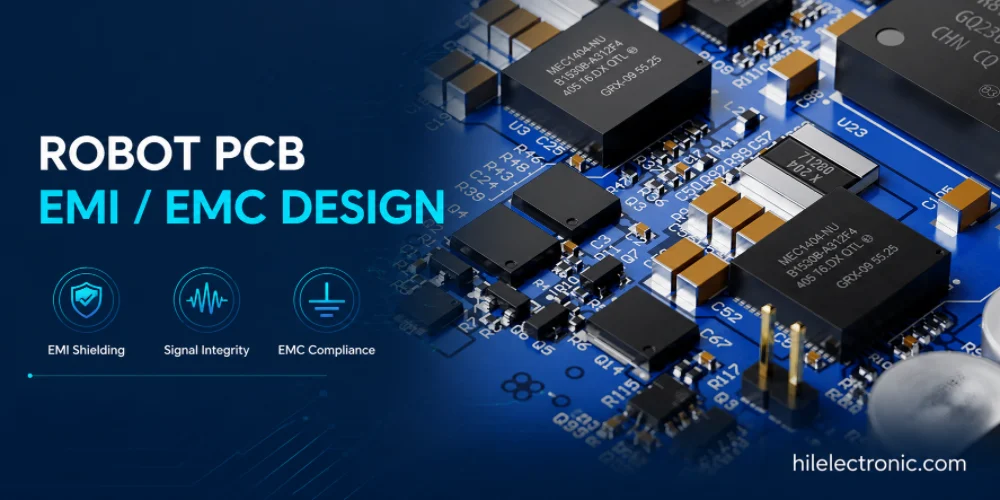
Robot PCB EMI/EMC Design for Reliable Robotics
Robot PCB EMI and EMC design affects whether a robot can...
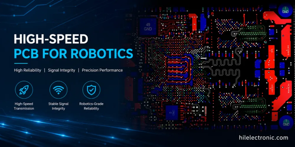
High-Speed PCB for Robotics: PCIe, DDR, MIPI and Ethernet Layout
High-speed PCB manufacturing for robotics supports data...
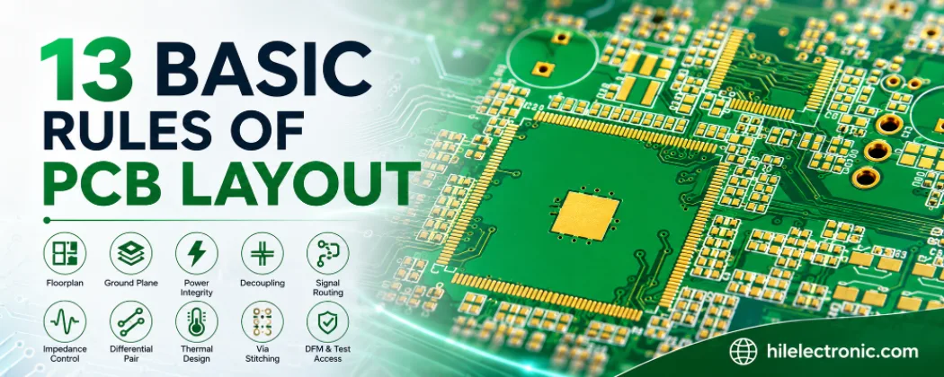
13 Basic Rules of PCB Layout (and the Failures They Prevent)
Figure 1. 13 Basic Rules Of Pcb Layout reference image for...

PCB Current Calculator: Sizing Trace Width and Vias with the IPC-2221 Formula
Figure 1. Pcb Current Calculator reference image for PCB...
How to get a quote for PCBs
Let us run DFM/DFA analysis for you and get back to you with a report.
You can upload your files securely through our website.
We require the following information in order to give you a quote:
-
- Gerber, ODB++, or .pcb, spec.
- BOM list if you require assembly
- Quantity
- Turn time
In addition to PCB manufacturing, we offer a comprehensive range of electronic services, including PCB design, PCBA (Printed Circuit Board Assembly), and turnkey solutions. Whether you need help with prototyping, design verification, component sourcing, or mass production, we provide end-to-end support to ensure your project’s success. For PCBA services, please provide your BOM (Bill of Materials) and any specific assembly instructions. We also offer DFM/DFA analysis to optimize your designs for manufacturability and assembly, ensuring a smooth production process.