
Back to blog
Advantages of Immersion Gold PCBs: A Comprehensive Guide

Out of all the intricacies that revolve around the manufacturing process of PCB, Immersion Gold PCBs are milestones achieved in terms of innovation and reliability. This article is trying to shed light on this advanced technology that is growing relevance perpetually to the world of modern electronics.
What is Immersion Gold PCBs
At its core, an Immersion Gold PCB refers to a type of PCB where the surface finish comprises a thin layer of gold, applied through a chemical deposition process. This gold layer, typically only a few microinches thick, is added over a copper substrate, ensuring a robust and highly conductive surface. The primary purpose of this gold coating is not just to “immortalize” the copper underneath but to provide a solderable surface for attaching various electronic components.
The significance of Immersion Gold PCBs in today’s electronics industry cannot be understated. From high-end consumer electronics to critical aerospace components, the presence of these PCBs is ubiquitous, marking a shift in how reliability and efficiency are perceived in electronic circuits.
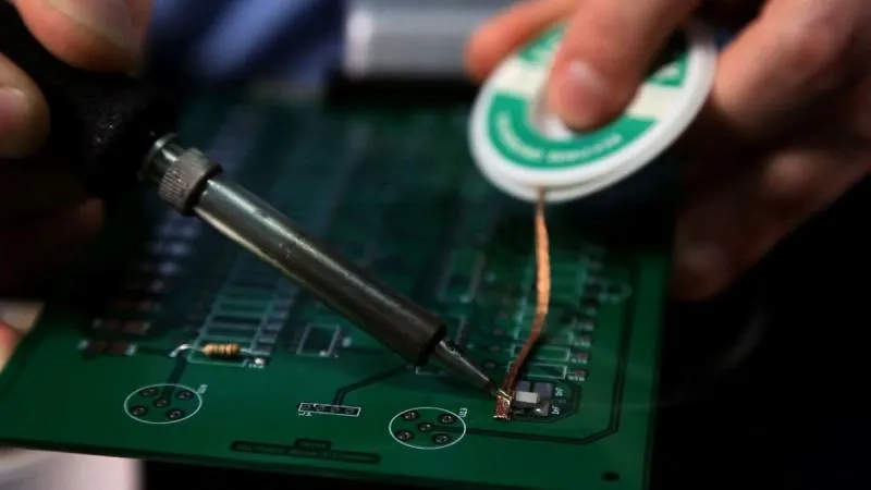
The Manufacturing Process of Immersion Gold PCBs
Immersion Gold PCBs, known for their reliability and superior performance, undergo a unique and intricate manufacturing process. This process not only sets them apart from traditional PCBs but also contributes to their enhanced qualities.
1. Preparing the Copper Substrate
The journey of an Immersion Gold PCB begins with the preparation of the copper substrate. This involves cleaning and ensuring the copper surface is free of any contaminants. The quality of the copper used is pivotal, as it forms the foundational layer upon which subsequent layers are built.
2. Applying the Copper Layer
A thin layer of copper is electroplated onto the substrate. This layer is crucial as it forms the conductive pathways for the PCB. The thickness of this layer can vary depending on the application requirements of the PCB.
3. Patterning the Circuitry
The next step involves patterning the circuitry on the copper layer. This is achieved through a process known as photolithography, where a photoresist material is applied to the surface and exposed to UV light through a mask, creating the desired circuit pattern.
4. Electroless Nickel Immersion Gold (ENIG) Coating
The ENIG coating process is a dual-layer metallic coating consisting of an electroless nickel layer topped with a thin layer of immersion gold. This process is critical in ensuring the longevity and functionality of Immersion Gold PCBs.
Nickel Layer Application
- The process starts with electroless nickel plating. This method does not use an electric current (as in electroplating) but relies on an autocatalytic reaction to deposit nickel on the copper substrate.
- Unlike electroplating, electroless plating ensures a consistent thickness of nickel across the entire PCB, regardless of its shape or density of the circuitry. This uniformity is crucial for the reliability of the final product.
- The nickel layer serves a dual purpose. First, it acts as a barrier to prevent copper from diffusing into the gold layer, which could otherwise lead to oxidation and corrosion. Second, it provides a robust and solderable surface for attaching electronic components.
Gold Layer Application
- Following the nickel plating, an immersion gold coating is applied. This is achieved by immersing the PCB in a bath containing gold salts, where a displacement reaction occurs. Gold, being a noble metal, replaces some of the nickel atoms on the surface.
- The gold layer in the ENIG process is typically very thin, usually between one to three microinches. This thinness is sufficient to protect the nickel layer from oxidation and to provide a good surface for soldering.
- The gold layer is not only resistant to oxidation and corrosion but also provides an excellent surface for wire bonding and a flat surface for placing small components and fine-pitch leads. Additionally, it is non-tarnishing and maintains its conductivity over time.
Quality Control in ENIG Coating
- Quality control is paramount in the ENIG process. The PCBs undergo rigorous inspection and testing to ensure the nickel and gold layers meet the required specifications in terms of thickness, adhesion, and uniformity.
- Common issues associated with ENIG, such as ‘black pad syndrome’ – a defect that leads to brittle solder joints, are meticulously monitored for. Advances in process control and chemistry have significantly reduced the occurrence of such issues.
5. Finalizing the PCB
The final steps involve etching away the unwanted copper and photoresist, inspecting the PCB for any defects, and applying any additional surface finishes or markings as required.
Comparative Analysis with Other PCB Surface Finishes
Compared to other surface finishes like HASL (Hot Air Solder Leveling) or OSP (Organic Solderability Preservatives), Immersion Gold PCBs offer superior durability and a flat surface, which is particularly beneficial for fine-pitch components.
The ENIG process, while more costly and complex than some other finishes, provides a level of reliability and conductivity that is unmatched, making it a preferred choice for high-reliability applications.
When the project moves from research to an RFQ, review PCB laminate selection and HDI stackup review so the material, process, and inspection requirements stay aligned.
Key Advantages of Immersion Gold PCBs
1. Enhanced Durability and Reliability
Robust Surface Finish: The gold layer in Immersion Gold PCBs provides a hard and durable surface, which is less prone to damage during handling and assembly. This durability translates to a longer lifespan of the PCB.
Reliable Solder Joints: The flatness of the surface finish ensures reliable solder joints, reducing the likelihood of defects in soldering, which is crucial for the overall reliability of the electronic device.
2. Superior Conductivity
Excellent Electrical Performance: Gold is known for its excellent conductivity. The thin layer of gold over nickel provides a superior conductive surface, essential for high-speed and high-frequency applications.
Consistent Signal Integrity: The uniformity of the gold layer aids in maintaining consistent signal integrity, which is vital for precision electronic devices.
3. Extended Shelf Life
Resistance to Oxidation: Gold’s resistance to oxidation is one of its most significant advantages. This property ensures that Immersion Gold PCBs can be stored for extended periods without degradation of the surface, unlike other finishes that may oxidize or tarnish.
Stable in Various Environments: These PCBs maintain their integrity in various environmental conditions, making them suitable for use in a wide range of applications, from consumer electronics to industrial and military equipment.
Applications of Immersion Gold PCBs
- From smartphones and computers to aerospace and medical devices, Immersion Gold PCBs are used in a myriad of applications. Their reliability and performance make them ideal for use in high-reliability products.
- In devices where precision and performance are non-negotiable, such as in satellite communication systems or advanced medical equipment, the use of Immersion Gold PCBs is often a standard.
- Preferred for Fine Pitch Technology: The flat surface provided by the Immersion Gold finish is particularly beneficial for fine-pitch technology, where component leads are very close together.
- Standard in High-End Electronics: Due to their superior qualities, these PCBs have become a standard in high-end electronics, where performance and reliability cannot be compromised.
In essence, the advantages of Immersion Gold PCBs—ranging from their durability to their exceptional conductivity and extended shelf life—make them an indispensable component in modern electronics. Their role in advancing the reliability and functionality of electronic devices is unmistakable.
Challenges in Using Immersion Gold PCBs
1. Higher Production Costs
The most significant challenge with Immersion Gold PCBs is their cost. The use of precious metals like gold and the complexity of the ENIG process make these PCBs more expensive than those with traditional surface finishes.
For large-scale projects or consumer electronics where cost-effectiveness is a priority, the use of Immersion Gold PCBs needs careful budgetary consideration.
2. Manufacturing Complexities
The ENIG process is sensitive and requires precise control of chemical concentrations, temperature, and timing. Any deviations can lead to defects such as the ‘black pad syndrome’.
Skill and Expertise Required: Maintaining consistency and quality in the ENIG process demands skilled labor and expertise, which can be a challenge for some manufacturers.
The Future of Immersion Gold PCBs in Electronics
- Expanding Applications:Broader Industry Adoption: As electronic devices become more sophisticated, the demand for reliable and high-quality PCBs grows. This will likely lead to broader adoption of Immersion Gold PCBs in various sectors, from consumer electronics to more specialized fields like aerospace and medical devices.
- Cost Reduction Strategies: One of the primary focuses for the future will be to reduce the costs associated with the ENIG process without compromising quality, making it more competitive with other surface finish technologies.
A Key Player in Technological Progress: As a crucial component in modern electronics, Immersion Gold PCBs are set to continue playing a key role in the advancement and reliability of electronic devices.
In summary, the future of Immersion Gold PCBs is one filled with potential and promise. Their continued refinement and adaptation will undoubtedly contribute to the growth and innovation in the electronics industry, making them a technology to watch in the coming years.
Choosing the Right Class for Your Needs
Assessing the Application Requirements
The nature of the final product’s application is the most critical factor. For electronics in life-critical systems, military, aerospace, or high-end medical devices where failure is not an option, Class 3 is the clear choice. For consumer electronics, home appliances, or less critical commercial products, Class 2 usually suffices.
Understanding the Cost Implications
Budget constraints cannot be overlooked. Class 3 manufacturing is more expensive due to its stringent quality requirements. If the budget is a major concern and the application does not demand extreme reliability, Class 2 might be the more economical choice.
Considering the Operating Environment
The environment in which the PCB will operate is another vital consideration. For harsh environments with extreme temperatures, vibrations, or moisture, Class 3 provides the necessary robustness. In contrast, for controlled environments with lesser demands, Class 2 is adequate.
Evaluating Long-Term Reliability and Maintenance
Think about the long-term implications. While Class 3 PCBs might be more expensive upfront, they could be more cost-effective in the long run due to their durability and lower maintenance needs. For products with shorter life spans or where regular upgrades are anticipated, Class 2 might be more appropriate.
Compliance with Industry Standards
Certain industries have specific requirements or standards that might necessitate the use of Class 3 PCBs. It’s important to be aware of these industry-specific regulations when making your decision.

Recommended Posts

ENIG PCB Surface Finish for Fine-Pitch Assembly
[pac_divi_table_of_contents...
Lead vs Lead-Free Soldering and Solder Melting Points in PCB
solder melting pointThe global electronics industry is...

Bulk Custom Aluminum LED PCB Manufacturing Services
After the mass production of aluminum PCBs is completed,...

Exploring PCB Surface Treatment: The Significance of ENIG and DIG
PCB Surface Treatment:ENIG PCB With the ever-evolving...